
A PCB, or printed circuit board, which is the pcb full form in electronics, is very important in the field of electronics. It acts like the backbone of electronic devices, connecting different parts and helping them work together. Understanding what PCB stands for in electronics allows you to appreciate its role in today’s technology. Over the last ten years, the use of PCBs has surged, with the market value expected to reach $92.4 billion by 2029. This growth highlights the significance of PCBs for both hobbyists and professionals alike.
Key Takeaways
PCBs, or printed circuit boards, are important for connecting electronic parts in devices like smartphones and computers.
Knowing how PCBs are built helps you see how they reduce complexity and make devices work better.
There are different types of PCBs, like single-sided, double-sided, and multi-layer. They are used for different purposes based on their design and complexity.
PCBs are very important in many industries. These include consumer electronics, industrial automation, and medical devices. They help ensure everything works reliably.
Learning about PCB technology can help you understand modern electronics better. It can also inspire you to explore more in this field.
PCB Definition
What is a Printed Circuit Board?
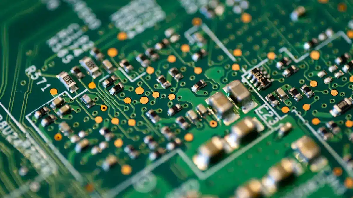
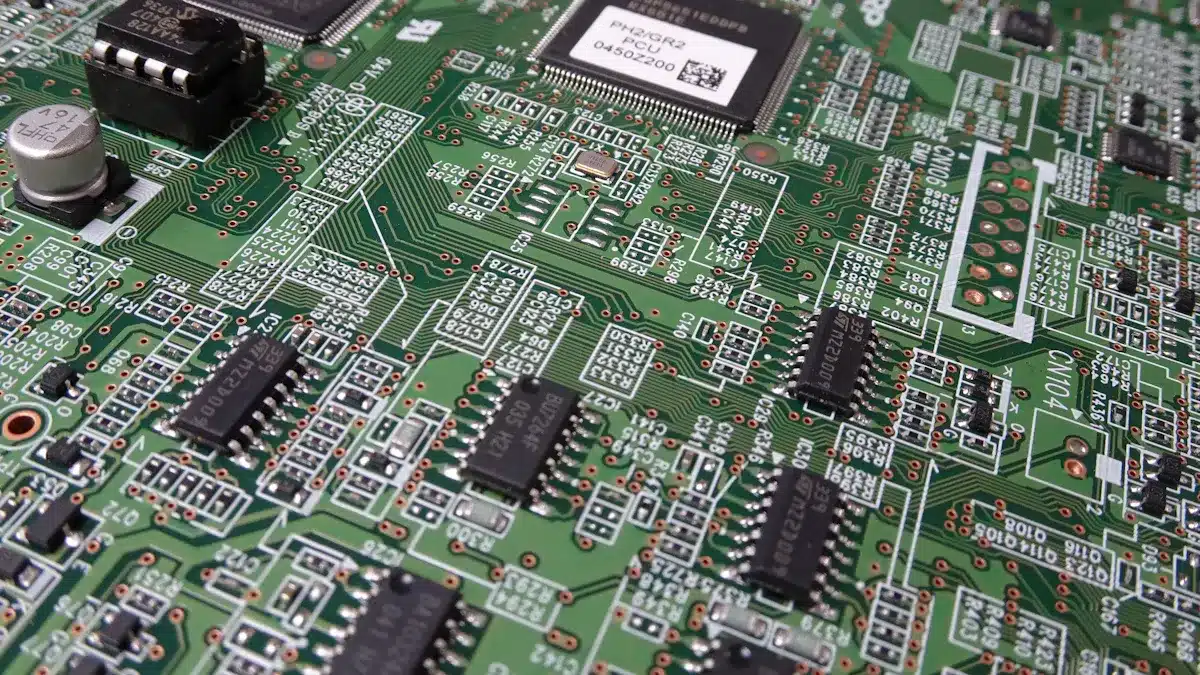
A printed circuit board (PCB) is an important part of electronics. The pcb full form in electronics means ‘Printed Circuit Board’. This board gives support and connects different electronic parts. You can find PCBs in nearly every electronic device, like smartphones and computers. They are the backbone that holds everything together.
PCBs are very important in electronic circuits. Here’s how they work:
Foundation for Electronics: PCBs are the base for most modern electronics. They give a stable place for parts to be attached.
Electrical Connections: Copper lines on the PCB create paths for electrical signals. These lines connect parts like resistors, capacitors, and integrated circuits (ICs).
Reduced Complexity: Using a PCB makes the design of electronic devices easier. This cuts down on complexity and space needed compared to manual wiring.
Making a PCB involves several steps:
Material Selection: A PCB is made from non-conductive materials, like fiberglass or epoxy.
Copper Traces: Thin layers of copper are etched onto the surface. These traces guide electrical signals between parts.
Component Mounting: Parts like resistors and capacitors are soldered onto the traces. This makes a strong connection for the device to work.
PCB Structure
Layers of a PCB
A printed circuit board (PCB) has many layers. Each layer has a special job. Knowing about these layers helps you see how PCBs work. Here’s a list of the main layers in a typical PCB:
Layer Type | Description |
|---|---|
Core | A solid material that does not conduct electricity. It is covered with copper where traces go. |
Copper Foil | This layer conducts electricity. The circuit design is printed here, leaving traces after etching. |
Signal Plane | This layer carries electrical signals between parts. It is designed to manage impedance. |
Power Plane | This layer spreads power supply voltages. It gives low-resistance paths for power across the PCB. |
Ground Plane | This layer gives a return path for electrical currents. It helps keep voltage levels stable. |
Prepreg | This is a material that isolates conductive layers from each other. |
Routing Layer | This layer is for routing electrical traces between parts. It is found between other layers. |
Copper Pour | These are copper-filled areas that help lower resistance and cut down interference. |
Silkscreen | The top layer shows where components go and has warnings. |
Solder Mask | This layer covers everything except the pads where components are soldered. It protects traces. |
These layers work together to make a working PCB. The conductive layers let electrical signals move. The insulating layers stop unwanted connections. This mix makes sure your electronic devices run well.
Materials Used
The materials in PCBs are very important for how they work. Common materials are:
FR-4 (fiberglass-reinforced epoxy resin)
Polyimide
Rogers (polymer-ceramic composites)
Aluminum
These materials give the needed electrical insulation and strength. For example, FR-4 is popular because it insulates well.
The way conductive and insulating materials work together is key. Copper pathways let electrical signals travel. Insulating materials like fiberglass support the board and stop short circuits. This balance helps your devices work right, ensuring they perform reliably.
Types of PCBs
When you look at printed circuit boards (PCBs), you will see three main types. They are based on how many layers they have: single-sided, double-sided, and multi-layer PCBs. Each type has different uses and special features.
Single-Sided PCB
A single-sided PCB has one layer of conductive material, usually copper. This design is simple and cheaper to make. Here are some important features:
Structure: It has a base layer with a conductive layer on one side. Components are placed on one side, while the conductor pattern is on the other side.
Applications: You can often find single-sided PCBs in:
Consumer electronics like calculators and remote controls.
Power supplies for simple circuits.
LED lighting systems because of their easy connections.
Automotive uses, like dashboard indicators.
Single-sided PCBs are great for low-density circuits, making them perfect for simple devices.
Double-Sided PCB
Double-sided PCBs have conductive material on both sides. This allows for more complex designs. This type can hold more components and has intricate routing. Here are some key points:
Design Complexity: You can place traces and components on both sides, which allows for compact designs.
Manufacturing Process: Making double-sided PCBs needs careful alignment and drilling of vias. This makes it more complicated than single-sided boards.
Applications: Common uses include:
UPS systems and power supplies.
Automotive dashboards and consumer electronics.
Double-sided PCBs are great for advanced applications that need compactness and high signal quality.
Multi-Layer PCB
Multi-layer PCBs have more than two layers of conductive material. They are important for complex devices that need more circuits than a single layer can hold. Here’s what you should know:
Complexity Handling: Multi-layer PCBs can support more circuits, allowing for greater power and speed for advanced uses.
Durability: Their thickness makes them more durable, so they can handle tougher conditions.
Applications: You will find multi-layer PCBs in:
Medical devices like MRI machines.
Consumer electronics such as smartphones and laptops.
Industrial electronics for automated systems.
Multi-layer PCBs provide more functions in a smaller space, making them perfect for modern technology.
PCB Applications
PCBs are very important in many industries. They help many devices work properly. Knowing how they are used helps you see their value in everyday technology.
Consumer Electronics
In consumer electronics, PCBs are essential. You can find them in many devices you use every day. Here are some common products that have printed circuit boards:
Smartphones
Tablets
Laptops
TVs
Gaming systems
These devices depend on PCBs to connect parts and allow communication. The need for better electronics pushes new ideas in PCB technology. As devices get smaller and more advanced, makers create new types like flexible and high-density interconnects. This change improves how well your favorite gadgets work.
Industrial Applications
PCBs are key in industrial automation and control systems. They form the base for electronic parts that run machines. You can think of PCBs as the nervous system of industrial tools. They help different parts talk to each other. This makes sure that complicated tasks happen smoothly and reliably.
Here are some important points about PCBs in industry:
They can handle tough conditions like heat, vibration, and moisture.
Different kinds of PCBs, like Flex and Multi-layer boards, solve specific problems in industry.
Choosing the right PCB improves machine reliability and lowers costs.
The design of trace width and spacing is very important for keeping signals clear. Exact sizes help keep sensitive signals accurate and reliable. This care is crucial for the smooth running of industrial systems.
Material Type | Key Properties | Applications |
|---|---|---|
Ceramic | High-temperature performance, excellent durability | High-end industrial applications |
Polyimide | High resistance to moisture and chemicals | Harsh environments |
FR-4 | Mechanical strength and durability | General industrial use |
Rogers/Teflon | Low dielectric constant, low loss tangent | High-frequency applications |
Medical Devices
PCBs are also very important in medicine. They help ensure accuracy, data processing, and reliability in medical devices. Here are some uses where PCBs are needed:
Cardiovascular Applications: Used in devices like pacemakers.
Medical Imaging: Essential for MRI machines.
Monitoring Devices: Found in body temperature monitors and other health gadgets.
You can find PCBs in diagnostic tools like X-ray machines and CT scanners. They are also key in patient monitoring systems like electrocardiogram (ECG) machines and blood glucose monitors. The reliability of these devices is very important because they affect patient care.
Also, rules and standards greatly affect how medical device PCBs are designed and made. Following these rules ensures safety and long-lasting performance. Knowing these needs is important for engineers and makers to create reliable medical products.
In short, printed circuit boards (PCBs) are very important for today’s electronics. They help connect electronic parts, allowing devices to work well. PCBs are key in making gadgets smaller and use less energy. Knowing how important they are helps you appreciate everyday tech, like smartphones and laptops.
You can learn more about PCB technology to see its many uses and benefits. This information is helpful for both fans and experts. Think about checking out materials that explain PCB design and uses. This will help you understand how these key parts influence the technology you use every day.
PCBs help make modern gadgets compact.
They improve how different devices work in many fields.
Understanding PCBs helps you appreciate tech progress.
FAQ
What is the main purpose of a PCB?
The main purpose of a PCB is to support and connect electronic parts. It gives a stable base for items like resistors and capacitors. This helps them work together well.
How are PCBs manufactured?
PCBs are made through several steps. First, designers create a layout. Next, manufacturers etch copper lines onto a non-conductive material. Finally, they attach parts and solder them in place.
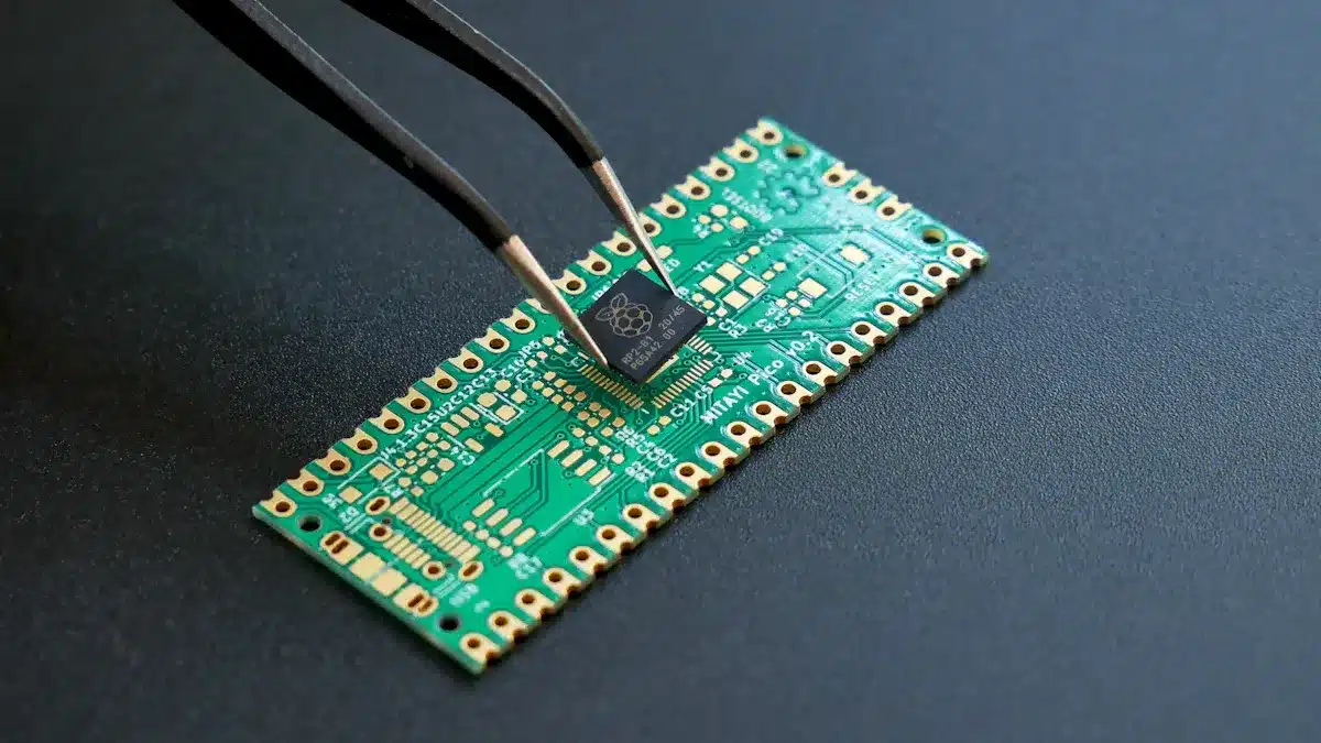
Can I make my own PCB at home?
Yes, you can make your own PCB at home! You can use DIY kits or software to design your layout. Then, you can etch the board using simple materials and methods.
What materials are commonly used in PCBs?
Common materials for PCBs include FR-4, polyimide, and aluminum. These materials provide electrical insulation and strength, ensuring reliable performance in many uses.
Why are multi-layer PCBs important?
Multi-layer PCBs are important because they allow for more complex circuits in a small space. They support advanced electronic devices, improving performance while saving space.
See Also
Understanding PCBA: Its Significance in Electronic Components
Decoding PCBA: Why It Matters in Electronics
Exploring PCBA: Its Definition and Function in Electronics