
Printed circuit boards (PCBs) are crucial in today’s electronics, serving as the backbone for many devices. They connect various components seamlessly. The pcb manufacturing process involves several detailed steps, including design, fabrication, assembly, and testing. As technology evolves in 2025, having a solid understanding of the pcb manufacturing process is essential for professionals in this field. Mastering this process can lead to innovative improvements and enhance the overall production of circuit boards.
Key Takeaways
Good PCB design begins with careful planning of schematics and layouts. This helps avoid signal and heat issues.
Picking the right materials and using better etching methods makes PCBs better and faster.
Surface Mount Technology lets us create smaller, quicker, and flexible PCB designs. Through-Hole Technology gives strong and lasting connections.
Testing methods like functional testing and automated optical inspection find problems early. This ensures PCBs are reliable.
Automation and new technologies make production faster. They also lower mistakes and help create new PCB designs in 2025.
PCB Design
The PCB design phase is very important in making PCBs. It has two main parts: schematic design and PCB layout.
Schematic Design
Schematic design is like a map for the printed circuit board. Engineers make a picture of the circuit. This shows how the parts connect. This step is very important because it affects how well the final product works. Some common problems during schematic design are:
Impedance changes and electromagnetic interference (EMI) from sudden trace width changes.
Noise in the power distribution network (PDN) that affects power supply circuits.
Wrong component placement, which makes routing harder and can cause signal issues.
Problems with heat management that can shorten component life.
Mechanical issues like board bending and layer misalignment.
To solve these problems, careful planning is needed. Engineers can keep impedance steady by routing traces wisely. They should also use thermal vias and high-Tg materials to manage heat well.
PCB Layout
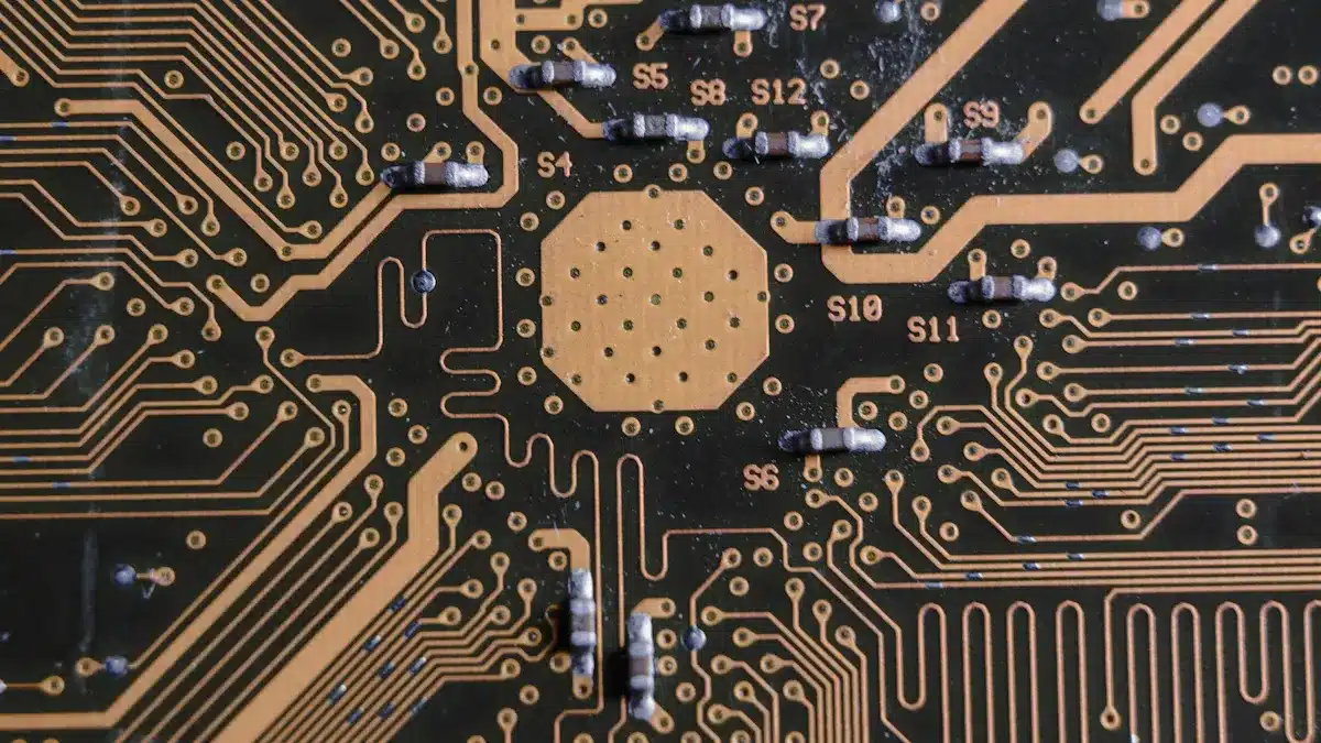
After the schematic is done, the next step is PCB layout. This means placing components on the board and setting up the electrical connections. A good layout helps signals flow well and reduces interference. Engineers must create design files for making the board, which includes making Gerber files. These files give detailed info about each layer of the circuit board, like copper traces, solder masks, and silkscreen layers.
PCB Fabrication
The PCB fabrication process has important steps. These steps change design files into working printed circuit boards. Two key parts of this process are choosing materials and the etching process.
Material Selection
Picking the right materials is very important for good PCB fabrication. The most common materials for PCB substrates in 2025 are:
FR-4: This is the top choice because it is cheap and works well (about $0.10 to $0.50 per square inch).
Rogers substrates: These are used for high-frequency needs, but they cost more (from $5.00 to $75.00 per square inch).
Ceramic substrates: These have great thermal conductivity (20-200 W/mK) and are good for high-power needs, costing between $2.00 and $10.00 per square inch.
Polyimide substrates: These work well in very hot places, with glass transition temperatures over 250°C.
PTFE (Teflon) substrates: They have great dielectric properties and stability, making them good for RF uses.
Flexible substrates: Materials like PET and polyimide are used for flexible designs. PET is cheaper but has lower glass transition temperatures (~80°C).
Composite epoxy materials: CEM-1 and CEM-3 are used for budget-friendly projects, with CEM-3 being cheaper for double-sided boards than FR-4.
Choosing the right substrate material affects how well the final circuit board works.
Etching Process
The etching process is very important for making circuit patterns on the PCB. New technology in etching has made this step faster and more accurate. Key improvements include:
Laser etching technology: This method helps PCB making by being precise, fast, and flexible. It does not use chemicals and allows for detailed designs.
Chemical-free etching processes: These eco-friendly methods, like water-based or dry etching, cut down on toxic waste and health risks.
Nano-enhanced etching solutions: Using nanoparticles speeds up etching, allowing for thinner lines and tighter tolerances.
Advanced etching equipment: Features like automated controls and real-time monitoring help make the process better and more consistent.
Green etching technologies: Methods like electrolytic and plasma etching reduce waste and energy use, helping the environment.
Layer alignment is very important during PCB fabrication. If layers are not aligned, it can cause defects and lower the quality of the circuit board. Recent reports say that alignment errors cause 18% of defects in multilayer PCB prototypes. However, new systems can lower defect rates by 15-25%, improving yield rates. Top manufacturers can reach up to 99.5% yield, with only 0.5% defects.
Optical inspection is key for checking layer alignment and quality. This process uses cameras and software to find any problems in the layers before assembly. By using strict optical inspection, manufacturers can find issues early, making sure the final product meets standards.
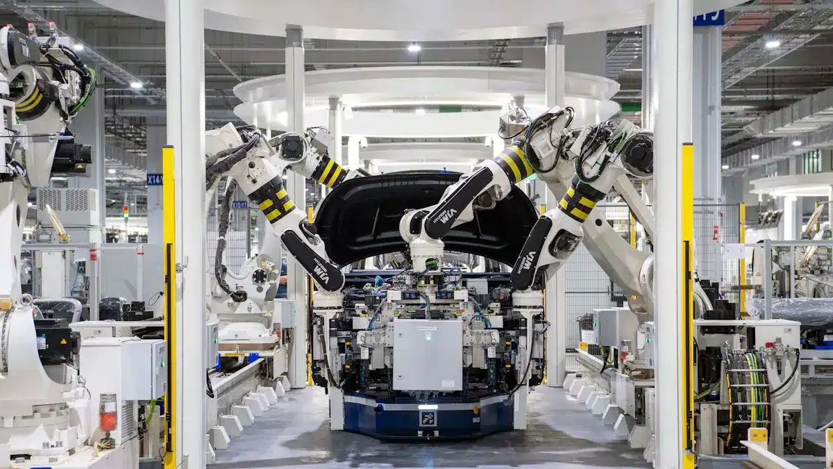
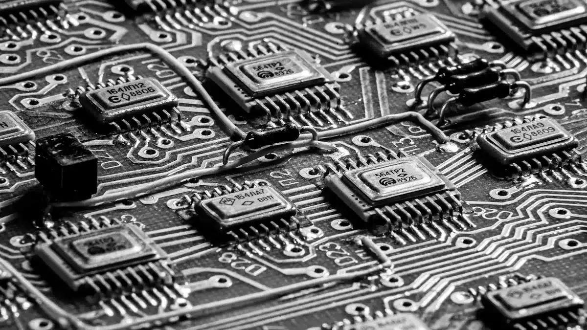
Circuit Board Assembly
The circuit board assembly process uses two main methods: Surface Mount Technology (SMT) and Through-Hole Technology. Each method has special features that affect how well the final product works.
Surface Mount Technology
Surface Mount Technology (SMT) lets us place parts right on the surface of the printed circuit board. This method has many benefits:
PCBs can be smaller and thinner because SMD components are tiny. This allows for compact designs.
There is more flexibility in PCB design and materials. This means we can create advanced types like Flex and Rigid Flex PCBs.
Material and handling costs go down because of the smaller size and no plated through-holes.
Production is easier because SMD components can be placed automatically without needing manual lead insertion.
High-frequency signals work better with less radio frequency interference and stronger anti-vibration properties.
But SMT also has some challenges. The initial costs are high because SMT equipment like reflow ovens and pick-and-place machines are expensive. Inspection can be hard due to the small size of components and hidden solder joints, which need costly inspection tools. Also, components can be sensitive to static and may get damaged easily, so careful handling is needed.
Through-Hole Technology
Through-Hole Technology means putting component leads into drilled holes and soldering them to the PCB. This method gives strong mechanical connections, making it good for high-power uses. Key benefits include:
Strong connections that can handle physical stress in tough environments like aerospace and automotive.
Better heat dissipation because through-hole components are larger, which helps them tolerate high temperatures.
Visible soldered connections make inspection and testing easier, improving product quality and reliability.
These mechanical and thermal benefits make Through-Hole Technology great for high-power PCB assemblies where durability is very important.
Both assembly methods are important in the PCB assembly process. Also, using solder masks and silkscreen printing improves the function and look of the circuit board. Solder masks protect the PCB from damage and stop solder bridges during assembly. Silkscreen printing gives important information, like component labels and logos, making assembly clearer and easier.
Testing and Quality Assurance
Testing and quality assurance are very important in the PCB manufacturing process. These steps make sure the final product works well and meets the needed standards. There are different testing methods, each with its own benefits and uses.
Functional Testing
Functional testing checks if the PCB works as it should. This means turning on the board and pretending to use it to find any problems. Here are some common functional testing methods:
Testing Method | Description | Key Characteristics and Usage |
|---|---|---|
Functional Testing (FCT) | Turns on the PCB and simulates use to check digital and analog signals with special software. | Finds circuit problems when powered; measures power use; needs complex and costly tools; ensures it works right. |
In-Circuit Testing (ICT) | Uses a special tester to check parts and solder connections without powering the board. | Looks for shorts, opens, resistance, capacitance; fixed probes; costly and less flexible; good for big connections and BGAs. |
Flying Probe Testing | A test that uses movable probes controlled by software without needing a fixture. | Flexible and adaptable; slower than ICT; great for prototypes and small batches; lower cost. |
Automated Optical Inspection (AOI) | Uses cameras and software to visually check for defects without contact. | Finds solder and component problems; no power needed; should be used with other tests; used at different stages of making. |
Burn-In Testing | Puts PCBs through electrical and heat stress to find early failures. | Continuous power or high heat exposure; finds early failures; may shorten PCB life if overstressed. |
X-Ray Inspection (AXI) | Uses X-rays to check hidden solder joints and internal traces, especially for dense SMT parts. | Finds hidden problems in BGAs and CSPs; needs skilled workers; takes time and is costly. |
Functional testing is key for spotting problems that could cause product failure. It helps makers ensure that each PCB meets performance standards before it goes to market.
Automated Optical Inspection
Automated Optical Inspection (AOI) has changed how quality is checked in PCB manufacturing. This method uses high-quality cameras and smart image processing to find defects very accurately. AOI can spot issues like misplaced components, wrong orientations, and soldering mistakes down to 0.01 mm.
The benefits of AOI include:
Early Detection: AOI checks real PCBs against design plans to find mistakes early. This stops bad boards from moving forward or being shipped.
High Accuracy: AOI can find almost 99% of defects when used at different production stages, greatly lowering the chance of bad PCBs reaching the market.
Speed and Efficiency: AOI can check up to 100 boards every hour, much faster than the 10-15 boards checked by hand. This speed improves overall production.
Detailed Reporting: AOI creates detailed reports on defects, helping manufacturers improve their assembly processes and cut down on repeated mistakes.
Even though AOI can be costly and complicated to set up, using it with other inspection methods creates a strong quality control system. This approach reduces the chance of bad PCBs and improves overall product reliability.
Knowing how PCBs are made is very important for people in electronics. Big changes, like making things smaller with High-Density Interconnect (HDI) technology and using flexible PCBs, will change the industry by 2025. Engineers need to understand these changes to make better designs and ensure they can be made easily. Automation is key for improving quality and speed. It helps place parts accurately and find problems quickly. By dealing with global supply chain issues and using local manufacturing, engineers can speed up production. In the end, understanding PCB processes well leads to more reliable products and quicker time-to-market.
FAQ
What is a PCB?
A PCB, or printed circuit board, is the base for electronic parts. It connects different parts of a device. This helps them work together properly.
Why is PCB design important?
PCB design is very important because it affects how well the final product works. A good PCB design reduces problems like signal interference and heat issues. This makes electronic devices more reliable.
What materials are commonly used in PCB fabrication?
Common materials for making PCBs include FR-4, Rogers substrates, and flexible substrates. Each material has special features that change performance, cost, and how it can be used.
How does surface mount technology differ from through-hole technology?
Surface mount technology (SMT) puts parts right on the PCB surface. This allows for smaller designs. On the other hand, through-hole technology puts component leads into drilled holes. This gives stronger connections.
What role does testing play in PCB manufacturing?
Testing makes sure that PCBs work correctly and meet quality standards. Methods like functional testing and automated optical inspection find problems early. This stops faulty products from being sold.
See Also
Emerging Developments in PCB And PCBA Design Techniques
Complete Overview Of The PCBA Manufacturing Procedures
Key Phases In The PCBA Production Workflow Explained