
A PCB, or printed circuit board, is very important in electronics. If you’re wondering what does PCB mean, it refers to a board that connects different electronic parts, helping them work together. The importance of PCBs is huge—they have changed the electronics world since the 1930s. By using small circuits instead of big wires, PCBs made devices smaller. Knowing what does PCB mean and how it works is key for anyone who likes electronics. It is the base of almost every electronic device you see.
Key Takeaways
A PCB is a flat board. It connects electronic parts. This makes devices smaller and easier to build.
PCBs give strong support. They also create clear paths for electricity. This helps devices work well and save space.
There are three main types of PCBs. Single-sided is for simple projects. Double-sided is for moderate complexity. Multi-layer is for advanced electronics.
Common PCB parts are resistors, capacitors, and integrated circuits. They all work together to control and manage electricity.
The PCB manufacturing process has several steps. These are design, etching, assembly, and testing. This ensures high-quality and working electronic boards.
What Does PCB Mean?
Definition of Printed Circuit Board
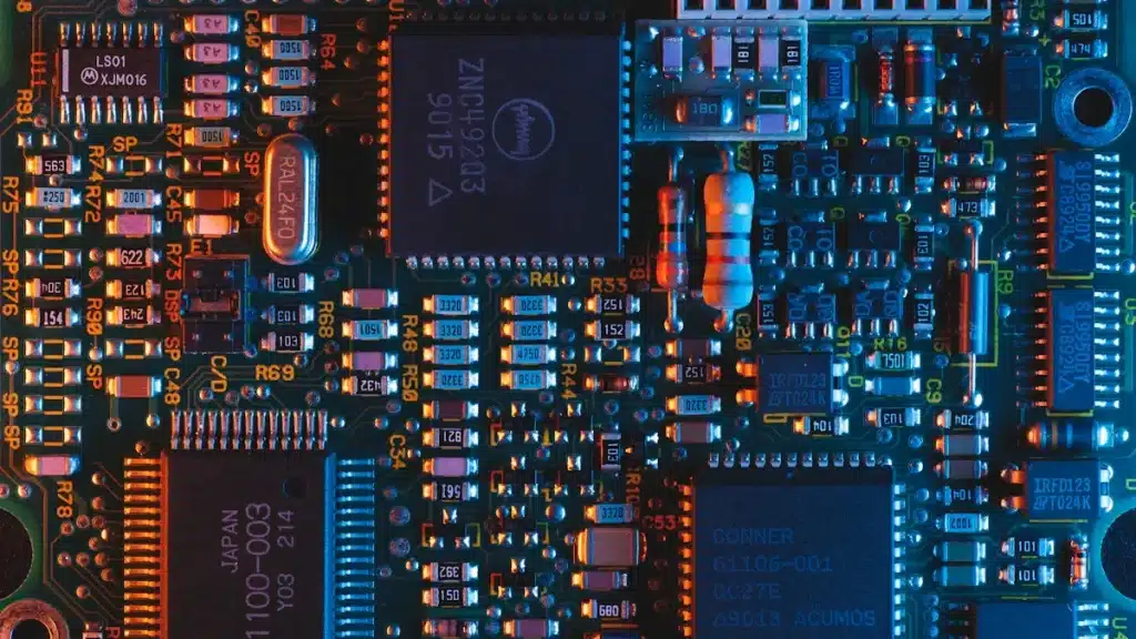
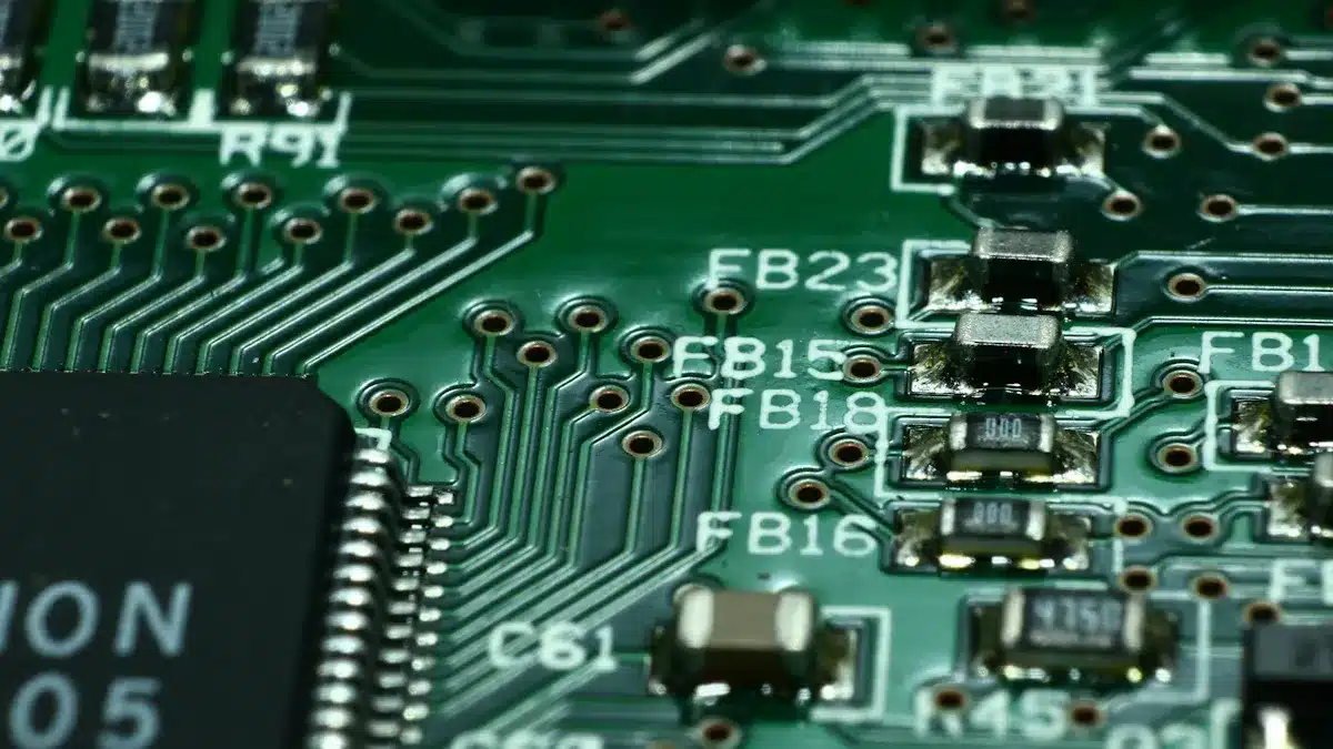
A printed circuit board (PCB) is a flat board. It is made from materials that do not conduct electricity, like fiberglass or plastic. The board has thin layers of copper traces on its surface. These traces are like roads for electricity. They connect different electronic parts, like resistors, capacitors, and integrated circuits. When you look at a PCB, you see a smart layout. This layout helps the parts work together well.
The design of a PCB is very important. It shows how the parts connect and work with each other. You can find PCBs in nearly every electronic device, from smartphones to computers. They are the main support for these devices, helping them work correctly. The goal of PCBs is to make it easier to put together electronic parts while keeping strong electrical connections.
Importance in Electronics
PCBs are very important in electronics. Here are some key reasons why they matter:
Mechanical Support: PCBs give a strong base for holding electronic parts. This support is important for keeping the device safe.
Electrical Connections: The copper traces on a PCB let electrical signals move between parts. This connection is essential for the device to work.
Reduced Complexity: Using PCBs makes wiring much simpler. Instead of many wires, a PCB neatly organizes connections. This saves space and cuts down mistakes.
Cost-Effectiveness: PCBs help make many electronic devices at once. This efficiency lowers production costs, making electronics cheaper for people.
Higher Functionality: Multi-layer PCBs can hold more complex circuits. This ability allows for better electronics with more features.
Types of Printed Circuit Boards
Printed circuit boards (PCBs) come in different types. Each type is made for specific uses and levels of complexity. Knowing these types helps you pick the right PCB for your project.
Single-Sided PCBs
Single-sided PCBs have one layer of conductive material, usually copper, on one side. This design limits how many parts you can use. It works well for simpler circuits. Here are some key features:
Conductive Layers: 1
Circuit Complexity: Simple
Cost: Low
Durability: Low
Flexibility: High
Typical Applications:
Consumer electronics like calculators and remote controls
Basic power supplies and LED lighting systems
Industrial controls and simple sensors
Single-sided PCBs are great for low-cost and simple projects. They are easy to make, which makes them popular with hobbyists and basic electronic devices.
Double-Sided PCBs
Double-sided PCBs have conductive layers on both sides. This design allows for more parts and higher circuit density. It is good for more complex uses. Here are some important features:
Conductive Layers: 2
Circuit Complexity: Moderate
Cost: Moderate
Durability: Moderate
Typical Applications:
Wireless sensors and motor controllers
Automotive electronics like dashboard indicators
Industrial controls that need moderate complexity
Double-sided PCBs help signals move faster and improve circuit performance. They allow better routing of signals through vias, which connect both sides of the board. This flexibility makes them good for devices needing advanced features.
Multi-Layer PCBs
Multi-layer PCBs have three or more conductive layers stacked together. This design allows for high component density and complex circuit layouts. Here are some key points:
Conductive Layers: 3 or more
Circuit Complexity: High
Cost: High
Durability: High
Typical Applications:
High-performance electronics like smartphones and computers
Medical devices and aerospace applications
Telecommunications equipment
Multi-layer PCBs have many benefits. They improve signal quality and reduce interference. They support miniaturization, which is important for small devices. Even though they cost more, they save money in the long run by needing fewer external parts.
Feature | Single-Sided PCB | Double-Sided PCB | Multi-Layer PCB |
|---|---|---|---|
Conductive Layers | 1 | 2 | 3 or more |
Circuit Complexity | Simple | Moderate | High |
Cost | Low | Moderate | High |
Durability | Low | Moderate | High |
Flexibility | High | Moderate | Moderate |
Typical Applications | Basic circuits, simple devices | Complex circuits, wearables, automotive | High-performance applications (smartphones, medical, automotive) |
Components of Printed Circuit Boards
Common Components
When you look at a printed circuit board, you will see many common parts. These parts are very important for how the board works. Here are some of the most used components:
Resistors: They control how much current flows in circuits.
Capacitors: They store and release electrical energy to filter signals.
Diodes: They manage the direction of current to ensure it flows right.
Transistors: They boost or switch electrical signals, acting like the brain of the circuit.
Integrated Circuits (ICs): They combine many functions into one chip, making devices smaller.
Connectors: They allow connections to other devices for communication.
Crystals and Oscillators: They give precise timing signals for synchronization.
Switches and Buttons: They let you control the current or events in the circuit manually.
Inductors: They store energy in magnetic fields and help with filtering.
Fuses: They protect circuits from too much current or voltage, preventing damage.
Electromechanical Components (Relays): These are switches controlled by electricity that manage larger currents.
Materials Used
The materials used to make printed circuit boards affect how well they work and how long they last. Here are some common materials:
Material | Key Properties | Typical Applications |
|---|---|---|
FR-4 | Fiberglass-reinforced epoxy resin; strong; good electrical insulation; stable in temperature | General purpose PCBs |
Rogers | Polymer-ceramic mix; great electrical performance; high thermal stability; good for high-frequency | High-speed, microwave circuits |
Metal Core | Aluminum or copper base; great thermal management; stable; lightweight | Power electronics, LED lighting |
Polyimide | Flexible; resists high temperatures and chemicals; lightweight | Flexible and rigid-flex PCBs |
These materials help your PCB handle the electrical and heat needs of modern electronics. For example, FR-4 is popular because it is cost-effective and reliable for many uses. On the other hand, Rogers materials are best for high-frequency uses, making them perfect for advanced communication devices.
Knowing these parts and materials will help you understand how printed circuit boards work in the electronic devices you use every day.
PCB Manufacturing Process
The PCB manufacturing process has several important steps. These steps change your ideas into working printed circuit boards. Each step is vital to make sure the final product is good quality and works well.
Design and Layout
The first step in making a PCB is the design and layout. You begin by deciding what the PCB will do and what it needs. This includes making a block diagram to show the circuit’s layout. Next, you create a detailed schematic that shows all parts and how they connect. After that, you choose parts and place them on the board. This placement affects how well the circuit works. Then, you connect the electrical paths, making sure signals stay strong. Finally, you check the design rules to ensure everything follows manufacturing standards. This careful process helps you make a reliable and easy-to-manufacture PCB.
Etching and Printing
Once the design is complete, the next step is etching and printing. This process removes extra copper from the board to create the circuit pattern you want. The most common way is wet etching, where chemical solutions like ferric chloride dissolve the unwanted copper. You can also use dry etching, which uses plasma to remove copper without chemicals. Laser etching is another choice, allowing for detailed and complex patterns. After etching, you add a protective layer to keep the desired copper areas safe during the process.
Assembly and Testing
The last step is assembly and testing. In large-scale production, you attach components using Surface Mount Technology (SMT) or Plated Through-Hole (PTH) methods. After placing the parts, you solder them in place. Automated Optical Inspection (AOI) checks for mistakes, ensuring correct placement and function. You may also run electrical tests to confirm the circuit works well. This careful testing process helps find and fix any problems before the PCB is sold.
By learning these steps, you understand how PCBs are made and why each stage is important for creating high-quality electronic devices.
PCB vs. PCBA
Definition of PCBA
A printed circuit board assembly (PCBA) is a PCB that has all its electronic parts added. This process includes soldering parts like resistors, capacitors, and integrated circuits onto the bare PCB. The PCB acts as the base with copper traces, while the PCBA becomes a working circuit that can do specific jobs. You can think of the PCB as the skeleton, and the PCBA as the complete body that can work in electronic devices.
Key Differences
Knowing the differences between a PCB and a PCBA is important for anyone interested in electronics. Here’s a quick comparison:
Aspect | Bare Printed Circuit Board (PCB) | Printed Circuit Board Assembly (PCBA) |
|---|---|---|
Definition | A bare board with copper traces and no components | PCB filled with electronic parts, making a working circuit |
Function | Gives mechanical support and electrical paths | Does specific electronic tasks |
Components | None (empty board) | Has resistors, capacitors, ICs, connectors, etc. |
Appearance | Flat board with conductive tracks, pads, and holes | Board with different electronic parts attached |
Manufacturing | Making it involves etching copper layers and adding solder mask | Assembly includes placing and soldering parts (SMT, through-hole) |
Testing | Checking for continuity and shorts in copper traces | Detailed testing including functional tests |
Stage | Base of the circuit | Finished and working electronic circuit |
Applications | Used in early design, prototyping, and circuit checks | Used in final products like smartphones, computers, and industrial electronics |
The change from PCB to PCBA has several steps. First, you put solder paste on the PCB where parts will go. Then, machines place the parts onto the board. After that, you heat the board in a reflow oven to melt the solder and make strong connections. Finally, you check and test the assembled board to make sure it works right. This process turns a simple PCB into a powerful PCBA that can work in many electronic devices.
In conclusion, printed circuit boards (PCBs) are very important in today’s electronics. They give support and connect different parts, helping devices work well. Here are some main points to remember:
PCBs allow for smaller and more efficient designs.
Their layered structure makes them strong in tough conditions.
Better manufacturing methods improve quality and lower failures.
As you use your electronic devices every day, think about the complex PCBs inside them. Knowing how important they are can make you more interested in electronics. You might want to learn more about PCBs and their new technologies to keep up in this exciting area!
FAQ
What is the lifespan of a PCB?
The lifespan of a PCB depends on the materials and how it is used. Usually, a good PCB can last between 10 and 20 years. Taking care of it and having the right environment can help it last longer.
Can I repair a damaged PCB?
Yes, you can fix a damaged PCB. You can change parts or repair broken paths using soldering. But if the damage is complicated, you might need a professional to help.
How do I choose the right PCB type?
Pick a PCB type based on what your project needs. For simple circuits, use single-sided PCBs. If your design is more complex, think about double-sided or multi-layer PCBs.
What are the common applications of PCBs?
PCBs are used in many different areas. Common uses include smartphones, computers, medical devices, and car electronics. They are important in nearly all electronic devices.
How do I design a PCB?
To design a PCB, start with a schematic diagram. Use PCB design software to arrange parts and paths. Make sure to follow design rules for making and working correctly.
See Also
Understanding PCB Design And Its Importance In Electronics
Exploring The Meaning Of PCBA And Its Electronics Role
Defining PCBA And Its Significance In Electronic Devices