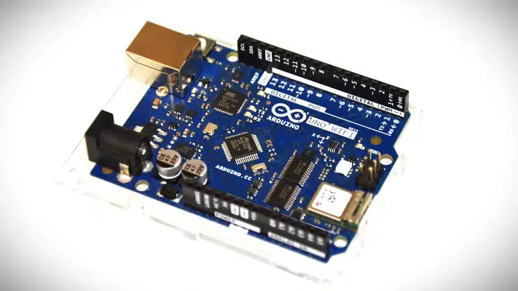

Printed circuit boards (PCBs), which stand for pcb board full form, are very important in today’s electronics. They are the main part of many devices. You use PCBs every day, like in smartphones and medical tools. They connect different electronic parts to work well. As technology grows, more PCBs will be needed. Knowing how important PCBs are can help you appreciate your devices more.
Key Takeaways
Printed circuit boards (PCBs) are very important. They connect electronic parts in devices like smartphones and medical tools.
There are different types of PCBs. These include single-sided, double-sided, and multi-layer designs. Each type has its own uses and functions.
Knowing about PCB structure and materials is helpful. This includes copper pathways and insulating layers. It helps us understand how they affect device performance.
Making PCBs involves many steps. This goes from design to assembly. These steps make sure the PCBs are reliable and work well.
The future of PCBs looks bright. Trends like miniaturization, better performance, and sustainability are changing the industry.
What is PCB?
A printed circuit board (PCB) is an important part of modern electronics. It connects electronic parts into one circuit. This setup lets electricity flow between parts. This helps devices work correctly. You can find PCBs in many devices, like smartphones and medical tools.
PCB Board Full Form
“PCB” means “printed circuit board.” This name shows how the paths connect different electronic parts. The printed part means putting conductive materials on a non-conductive base. This makes the needed connections.
Structure of a PCB
The structure of a PCB has layers and materials that support electronic parts. Here are the main materials used to build a PCB:
Prepregs
Laminates
Copper Foil
Soldermask
Silk Screen
Surface Finish
Prepreg is a material made from glass fabric with resin. It gives mechanical support to the PCB. Laminates form when you heat and press prepreg and copper foil together. This creates the main structure of printed circuit boards. Soldermask keeps copper tracks safe from oxidation. Silk screen adds labels on the PCB surface. Surface finishes help solder stick to exposed copper pads.
The layers of a PCB are very important for its performance. Each layer has a special job, like conducting electricity or providing insulation. Moving from single-layer to multi-layer designs allows for smaller and more powerful devices. More layers mean higher component density and better electromagnetic interference (EMI) shielding. A good stack-up design is key for better signal quality and controlling impedance.
Here’s a table showing the main functions of a printed circuit board in electronic devices:
Function | Description |
|---|---|
Mechanical Support | Gives a strong base for parts, keeping them in place and safe from stress. |
Electrical Connectivity | Makes paths for signals, sets up power networks, and allows fast transmission. |
Thermal Management | Moves heat away from parts and includes cooling solutions to avoid damage. |
Signal Integrity Preservation | Keeps signal quality high through controlled impedance and shielding from interference. |
Miniaturization Enablement | Helps create compact designs with advanced connection methods and flexible PCB options. |
Knowing how PCBs are built and what they do helps you see their importance in the devices you use every day.
Common Components of Printed Circuit Boards
Printed circuit boards (PCBs) have many important parts. These parts work together to make sure everything works well. Knowing about these parts helps you understand how PCBs function in electronic devices.
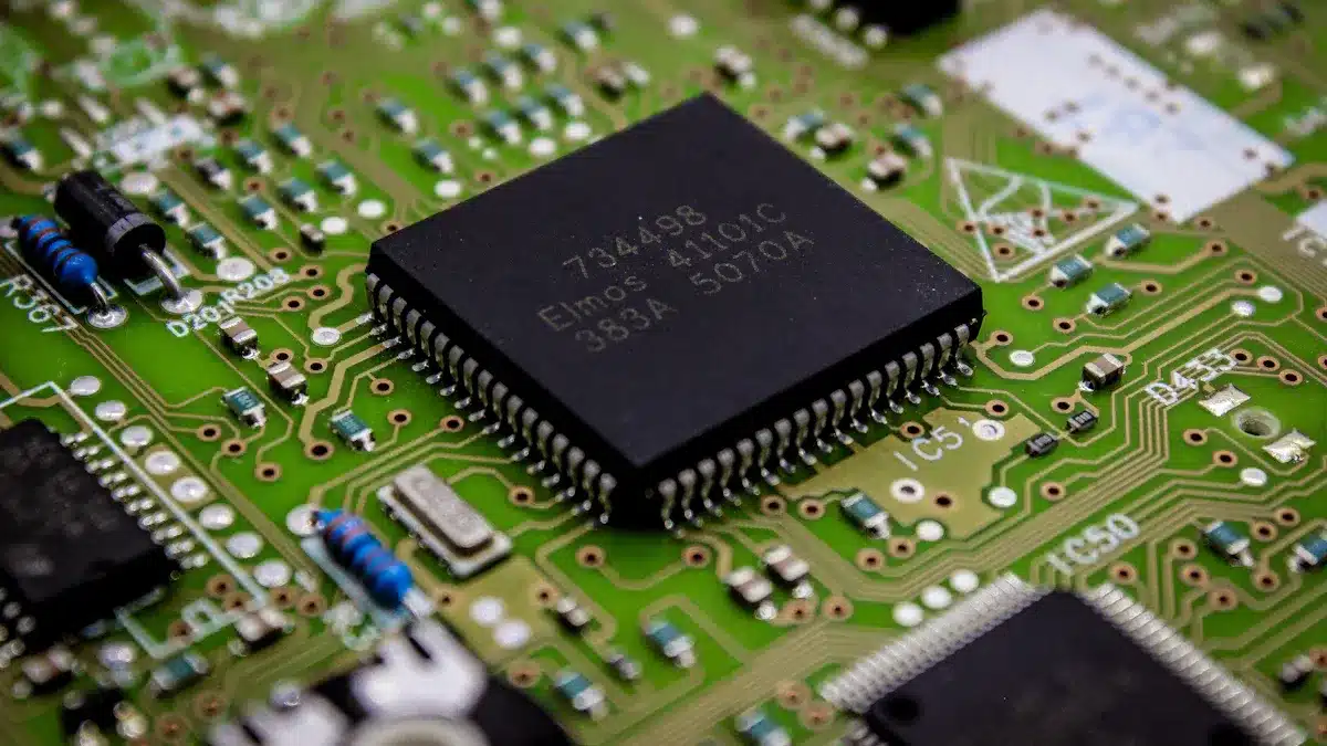
Conductive Pathways
Conductive pathways are very important for a printed circuit board. These pathways are mostly made of copper. They act like roads for electrical signals. They connect different parts on the board to create complete circuits. Here are some key jobs of conductive pathways:
They guide electrical signals between parts like resistors and capacitors.
They make things simpler and take up less space than manual wiring.
They help electrical current flow well between parts.
Conductive pathways are etched onto the board’s surface. This creates a network for accurate signal routing. This design lowers resistance and increases conductivity. Without these pathways, your electronic devices would not work well.
Insulating Layers
Insulating layers are very important for printed circuit boards. These layers stop unwanted current paths. This helps prevent shorts and cuts down on signal interference. Here are some key jobs of insulating layers:
Electrical Isolation: They keep electrical signals safe by keeping voltage and current in their paths.
Thermal Protection: Insulating layers help control heat. They stop heat from reaching sensitive areas and lower the chance of warping or delamination.
Mechanical Stability: They give support to the board, keeping it strong and absorbing vibrations. This is important in tough environments.
By keeping electrical signals safe and protecting against heat, insulating layers make PCBs last longer and work better. This protection is very important for your electronic devices.
Common PCB Layers
Printed circuit boards (PCBs) can have different layers. Each type has its own purpose and use. Knowing about these common PCB layers helps you see how they work in different devices.
Single-Sided and Double-Sided Layers
Single-sided PCBs have parts on one side. The other side has conductive pathways. These boards are simple and cheap. You often find them in basic electronics like calculators and cameras.
Double-sided PCBs have conductive layers on both sides. They connect parts using through-holes or surface mounts. This design allows for more complex circuits. You can see double-sided PCBs in devices like LED lights and vending machines.
Here’s a quick comparison of single-sided and double-sided PCBs:
Type of PCB | Layers | Description | Applications |
|---|---|---|---|
Single-Layer | 1 | Parts on one side, conductive pattern on the other. | Simple devices like calculators. |
Double-Sided | 2 | Conductive layers on both sides, connected via through-holes or surface mounts. | Intermediate complexity devices. |
Multi-Layer PCBs
Multi-layer PCBs stack several double-sided boards. They use vias to connect the layers, allowing for complex routing. More layers help reduce signal interference and improve power distribution. You usually find multi-layer PCBs in advanced electronics like computers and smartphones.
The number of layers in a PCB affects how it works. For example, two-layer boards are good for simple devices. Boards with six to twelve layers are common in cars and communication systems. Complex devices often need PCBs with twenty or more layers for the best performance.
Applications of Printed Circuit Boards
Printed circuit boards (PCBs) are very important in many industries. They are especially crucial in consumer electronics and medical devices. You see PCBs every day, often without knowing how important they are.
Consumer Electronics
In consumer electronics, PCBs are a must-have. About 70% of all printed circuit boards are used here. You can find PCBs in devices like:
Smartphones
Televisions
Laptops
Gaming consoles
Home appliances
These devices need PCBs to connect parts and work properly. For example, in smartphones, the PCB connects processors, memory chips, and other parts. This helps them communicate and do tasks. High-Density Interconnect (HDI) technology lets more parts fit into smaller spaces. This is very important for modern smartphone design.
Medical Devices
PCBs are also very important in the medical field. They help power and connect many medical devices. This ensures they give accurate readings and work reliably. Some common medical devices that use PCBs are:
Electronic Thermometers
MRI Machines
Blood Glucose Monitors
Implantable Cardioverter-Defibrillator (ICD) Devices
Healthcare Mobile Technology
These devices rely on PCBs to function. For instance, MRI machines use complex PCBs to process images. Blood glucose monitors depend on PCBs for accurate readings. The reliability of these devices can directly affect patient care. This makes PCBs essential in healthcare.
Manufacturing Process of PCBs
Making printed circuit boards (PCBs) has many important steps. Each step is key to making sure the final product works well. Here’s a simple list of the main steps in making PCBs:
Imaging and Printing the Design
Creating the Substrate
Printing the Inner Layers
Ultraviolet Light Blasting
Removing the Unwanted Copper
Layer Alignment and Inspection
Laminating and Bonding the Layers
Drilling
PCB Plating
Outer Layer Imaging
Tin Plating
Final Etching
Solder Mask Application
Silkscreening
Surface Finish
Testing
Profiling
Final Quality Check
Design and Prototyping
The design and prototyping stage is very important for making good PCBs. In this step, you create a model of the circuit board. This model helps find problems before making many boards. Here are some benefits of this step:
Finding and fixing design problems early saves time and money.
Better product performance by testing for real-world use.
Increased reliability by checking prototypes in different situations.
Aspect | Description |
|---|---|
Accuracy and Reliability | Prototypes help find design problems early, making sure the final PCB works as it should. |
Reduced Costs | Finding mistakes before production cuts down on expensive errors in the final PCB making. |
Etching and Assembly
After the design step, the etching and assembly steps start. Etching takes away unwanted copper to make the right circuit pattern. Common ways to etch include chemical and laser etching. Each way has its benefits, like being precise and easy to check.
During assembly, workers put parts onto the PCB. A good assembly process makes sure the solder joints are strong and stable. This is very important for the PCB’s reliability. Many makers use advanced testing during assembly. This helps find possible problems early, making the PCB more reliable.
Printed Circuit Boards (PCBs) are very important in today’s electronics. They are the base for putting together and connecting parts in many devices. You use PCBs every day, like in smartphones and medical tools. Their importance shows how complex and innovative technology is now.
In the future, the global PCB market is expected to grow a lot, reaching $92.4 billion by 2029. This growth comes from new technology and the increasing need for electronic devices. Some key trends are:
Miniaturization: Smaller, packed PCBs for tiny devices.
Higher Performance: PCBs made for faster frequencies and more power.
Sustainability: A move towards eco-friendly materials and methods.
As you learn about electronics, remember that PCBs are key for working in many fields. Their flexibility and innovation will keep changing the future of technology. 🌍
FAQ
What materials are used to make PCBs?
PCBs usually use copper for pathways, fiberglass for the base, and resin for insulation. These materials help make them strong and work well with electricity.
How do PCBs affect device performance?
PCBs connect electronic parts, helping them work together. A good PCB improves signal quality, cuts down interference, and makes devices more reliable.
Can I repair a damaged PCB?
Yes, you can fix a damaged PCB. You can solder new parts or use conductive ink for small problems. But, if the damage is serious, you might need a professional.
What is the lifespan of a PCB?
The lifespan of a PCB depends on how you use it and the environment. Usually, a good PCB can last many years, often over ten years in stable conditions.
How do I choose the right PCB for my project?
To pick the right PCB, think about size, number of layers, and how many parts it needs. Look at your project’s needs and ask manufacturers for help.
See Also
Understanding PCBA Motherboards: Their Function and Significance
Defining PCBA in Electronics: Importance and Applications
The Significance of PCBA in Electronic Circuits Explained
Exploring PCB Design: Its Importance in Electronic Engineering