The best way to approach manufacturing printed circuit boards depends on the complexity of the project. It also hinges on the required performance, cost, and reliability. Multilayer and high-density interconnection printed circuit boards dominate the global market, especially in advanced electronics like smartphones and aerospace systems. Rigid printed wiring boards account for 85% of the market share, while flexible printed wiring boards are rapidly growing due to innovative manufacturing methods. Key factors to consider in manufacturing printed circuit boards include design complexity, intended application, budget, reliability, and production volume. Choosing the right manufacturing printed circuit board process enhances electronic device quality and supports the growth of the electronics industry.
Key Takeaways
Pick PCB types and ways to make them by looking at how hard your project is, how much it costs, and how well it needs to work.
Talk with manufacturers early so you do not make mistakes, spend too much, or get bad boards.
Use multilayer, HDI, or flexible PCBs for small things, fast devices, or when you do not have much space.
Save money and get good boards by making simple designs, picking common materials, and buying more at once.
Check and test PCBs well with new tools to make sure they work and last a long time.
Key Factors for PCB Selection
Complexity and Design
How complex the design is affects which manufacturing technique is used. Devices are getting smaller and smarter, so designers use multi-layer boards and tiny spaces between parts. These features need special processes that can handle tricky layouts and special vias.
More complex designs need careful alignment and extra lamination steps.
Some layouts use covered or filled vias to lower defects and make assembly better.
The width and space of traces change how easy it is to make a pcb and how much waste is left over.
Designers and manufacturers work together to make sure the pcb fits both design and making needs.
Making the design simpler can save money and make the pcb more reliable.
Performance and Reliability
Performance and reliability matter for every electronic device. Putting power semiconductor devices inside a pcb makes converters smaller and helps with heat. This makes devices work better and last longer.
Good practices include placing parts carefully, using heat sinks and vias for cooling, and picking strong materials like FR4 or polyimide.
Following rules like IPC or UL helps the pcb work well and last longer. Using flexible or rigid-flex boards and lead-free soldering can also make devices more reliable.
Cost and Volume
Cost and how many pcbs are made are important when picking a method.
Making only a few pcbs costs more because of setup fees.
Making lots of pcbs lowers the cost for each one.
Small pcbs can cost more because panels are not used well and special processes are needed.
Handling and testing small boards can also raise costs.
To save money, designers can make circuits simpler, use common materials, and order more at once. The best method finds a balance between cost, quality, and reliability.
Application Needs
What the pcb will be used for decides the type, materials, and process. The choice of materials depends on how the pcb needs to handle electricity, movement, and heat. FR-4 works well for most home electronics, while high-frequency laminates are better for telecom devices. Metal-core boards help with heat in cars and power tools. Flexible and rigid-flex materials are good for wearables and aerospace electronics.
Certifications like ISO 9001 and RoHS show the pcb is safe and meets rules for the environment. Picking the right materials and process for the job makes sure the device works well and lasts.
Printed Circuit Board Types
Single-Sided PCB
Single-sided printed wiring boards have one copper layer. This layer sits on a base that does not conduct electricity, like fiberglass or phenolic resin. These boards are simple and cheap to make. They are used for circuits that are not very crowded or hard to build. You can find them in things like calculators, remote controls, LED lights, and power supplies. Since there is only one layer for parts, these boards cannot hold many pieces. They work best in simple electronic devices.
Aspect | Common Use Cases and Limitations | |
|---|---|---|
Conductive Layers | One copper layer | Good for easy circuits |
Substrate Material | Fiberglass or phenolic resin | Used in home electronics and factory controls |
Cheap to make | Not good for hard designs | |
Applications | Calculators, LED boards, car parts | Not much space and no way to cross traces |
Double-Sided PCB
Double-sided printed wiring boards have copper on both sides. This lets people make more paths and add more parts. Vias connect the two sides, so traces can cross and more pieces fit. These boards are good for circuits that are a bit harder, like LED drivers, vending machines, car dashboards, and phone systems.
Feature | Single-Sided PCB | |
|---|---|---|
Only one side | Both sides | |
Easy | Medium | |
Cost | Cheaper | Costs a bit more |
Applications | Calculators, printers | Car dashboards, factory controls |
Multilayer PCB
Multilayer printed wiring boards have many layers stacked together. This helps fit lots of parts and do more things. When surface-mount and microvia technology became popular, these boards got used more. Now, multilayer PCBs are everywhere, like in computers, phones, medical tools, and military radios. They are important for today’s electronics because they can do a lot and work well.
Note: Multilayer printed circuit boards are the biggest part of the world market. They are used in phones, cars, planes, and home electronics.
HDI PCB
High-Density Interconnect (HDI) printed wiring boards use tiny holes and thin lines. These help make small and powerful devices. HDI PCBs are used for things like 5G, IoT, and AI. They send signals better, lower noise, and last longer. Makers use HDI PCBs in smart gadgets, medical tools, and car electronics.
Small size lets devices be tiny but strong.
Thin lines help send fast signals.
HDI PCBs cost less to put together in big amounts.
Better layouts help cool parts and make them last.
Needed for new and smart electronic features.
Flexible and Rigid-Flex PCB
Flexible and rigid-flex printed wiring boards can bend and also stay stiff. This means fewer connectors and wires are needed, so they save space and weight. These boards can handle bumps, shakes, and tough places. They are used in medical tools, planes, the army, cars, and home electronics because they last long and can do many things. Wearables, fitness bands, and robots use these boards because they are small and strong.
Manufacturing Printed Circuit Methods
Subtractive Process
The subtractive process is the most used way to make printed circuit boards. In this method, makers start with a board covered in copper. They use a chemical etching manufacturing process to take away copper they do not need. Only the wanted circuit pattern stays on the board. This works well for hard boards like FR4. It is good for making many boards at once and gives steady results. The subtractive process can make big holes without copper, and it does not need extra drilling. But it cannot make big plated holes unless welding rings are used. It also has trouble with thick copper layers.
Additive Process
The additive process uses a different manufacturing process. Instead of taking copper away, it adds traces by putting down conductive ink or plating copper right onto the board. This way works with more types of materials, like flexible and curved boards. The additive process is good for quick testing and fast design changes. It is best for flexible hybrid electronics and small batches. Makers must make sure the plating sticks well to the board so it works right.
Key differences between subtractive and additive manufacturing processes:
Aspect | Subtractive Manufacturing | Additive Manufacturing |
|---|---|---|
Process | Removes copper from substrate via chemical etching | Deposits conductive ink onto substrate to build traces |
Materials | Limited to rigid substrates like FR4 or Kapton | Supports rigid, flexible, and curved substrates |
Equipment & Chemicals | Uses harsh chemicals and specialized machinery | Uses conductive ink printing technology, often desktop printers |
Production Suitability | Optimized for mass production, mature industrial process | Ideal for rapid prototyping and flexible scaling |
Lead Time & Flexibility | Longer lead times, less flexible for quick design changes | Fast iteration, prototyping at desk possible |
Applications | Suited for rigid PCBs with powerful silicon components | Enables flexible hybrid electronics and new form factors |
Lamination and Drilling
Lamination is the main step for making multilayer boards. Makers stack inner layers, prepreg, and copper foil in a set order. They use pins to keep the stack lined up. Then, they use heat and pressure to melt the resin and stick all the layers together. After it cools, the stack becomes one strong board. Foil lamination uses copper foil for the outside layers and works for most boards. Cap lamination is used when blind vias or special materials are needed.
Drilling comes after lamination. Fast machines drill holes for through-hole vias. For blind and buried vias, drilling is done before lamination. Laser drilling makes tiny micro-vias for high-density boards. After drilling, makers add a thin copper layer to the hole walls. This helps make sure the holes can carry electricity.
Plating and Surface Finishing
Plating and surface finishing help protect the pcb and make it work better. Makers control how thick the plating is to keep it strong and able to carry electricity. They pick materials like gold, silver, tin, or nickel for different uses. Good sticking between the plating and the board stops peeling. Even plating keeps signals strong and steady. Surface finishes like HASL, OSP, ENIG, and immersion silver each have their own good points. ENIG gives a flat, tough surface for high-performance boards. OSP is good for short-term or small runs. Quality checks, like looking at the board and measuring thickness, help keep every manufacturing process at a high standard.
PCB Assembly Techniques
Surface-Mount Technology
Surface-mount technology changed how printed circuit boards are made. It lets engineers use smaller and lighter parts. Parts can go on both sides of the board. This saves space and makes more connections. SMT helps make assembly faster and uses machines. This lowers work and costs. Key benefits of SMT include:
Parts are small and light, so boards are compact.
More connections fit for advanced electronics.
Both sides of the board can hold parts.
Machines make assembly quick and cheap.
Boards work well even when they shake or move.
SMT is used in most new electronics. It helps make devices small, light, and strong. But SMT is not good for places with lots of shaking or force.
Through-Hole Assembly
Through-hole assembly is still important for tough jobs. This method uses parts with leads that go through holes. This makes strong connections. Situations where through-hole assembly works best:
Boards last longer when there is shaking or heat.
Used in military, planes, and cars.
Good for testing because parts can be changed.
Handles heat well for power electronics.
Connections are easy to see and check.
Through-hole technology is good for hard places. But it takes more time and costs more than SMT.
Embedded Components
Putting parts inside the board helps make smaller and stronger boards. This keeps signals clear and protects parts from damage.
Aspect | Advantages | Challenges |
|---|---|---|
Boards get smaller for tight spaces. | Cavities must be the right size or boards can fail. | |
Signal Integrity | Short paths help signals move fast. | Testing is harder after parts are inside. |
Reliability | Parts are safe from heat and shaking. | Only some passive parts can be used this way. |
Cost Efficiency | Saves money when making lots of boards. | Costs more at first and needs special steps. |
Fabrication Complexity | Special lamination puts parts inside. | Not every maker can do this. |
Thermal Management | Ways to cool parts are used. | Cooling is harder for parts inside the board. |
Testing and Repair | Tests and checks make sure boards work. | Fixing parts is hard or not possible after making. |
Engineers need to think about these pros and cons before using embedded parts.
Automated Assembly
Automated assembly is key for making boards fast and well. Machines put parts on boards quickly and correctly. This means fewer mistakes and more boards made.
Automated Process | Impact on Efficiency and Quality |
|---|---|
Pick-and-place machines work fast and make fewer mistakes. | |
Solder Paste Printing | Machines put solder on evenly, so boards have fewer problems. |
Automated Inspection | AOI and X-ray machines find problems early and keep boards working well. |
Automation lets factories work all day and night. They can make lots of boards and change designs fast. This saves money and keeps quality high.
Testing and Quality Control
Non-Destructive Testing
Non-destructive testing helps keep electronic devices working well. Engineers use these tests to check printed circuit boards without breaking them. These tests find problems early and make devices more reliable. The table below lists common non-destructive testing methods and what they do:
NDT Method | Purpose / Application | Key Advantages / Notes |
|---|---|---|
X-ray Inspection | Looks inside to check solder joints under BGAs and QFNs | Finds hidden problems like voids and misaligned parts; needed for multilayer PCBs and important uses |
Ultrasonic Inspection | Checks through-hole soldering and solder quality in multilayer PCBs | Good for checking inside solder joints |
Infrared Thermal Imaging | Spots heat problems and uneven heat on the board | Finds faults caused by bad heat flow |
Visual Inspection | Uses cameras to spot surface problems like missing parts or solder bridges | Finds easy-to-see problems early; simple and cheap |
Automated Optical Inspection (AOI) | Uses cameras to find surface problems after solder paste and part placement | Catches missing parts, solder bridges, and polarity mistakes; helps stop defects |
Solder Paste Inspection (SPI) | Checks if solder paste is the right amount and in the right place | Makes sure solder covers well for strong connections |
Electrical Testing | Tests for connection, resistance, and capacitance problems | Checks if the PCB works right without hurting it |
In-Circuit Testing (ICT) | Uses probes to test each part’s function | Fast and accurate; great for making lots of boards; needs good design for testing |
Flying Probe Testing | Uses moving probes for small batches or prototypes | No special tools needed; flexible; slower than ICT but good for a few test points |
Boundary Scan Testing | Tests digital connections using IEEE 1149.1 standard | Checks connections without touching; good for high-density PCBs with BGAs |
Environmental Stress Screening (ESS) | Puts PCBs through heat, humidity, and shaking to find early failures | Speeds up aging to show weak spots like solder cracks |
Thermal Cycling | Changes temperature over and over to test strength | Shows how PCBs handle real-life heat changes; important for cars and planes |
Burn-in Testing | Runs the board hot for a long time to find hidden problems | Finds early failures; helps make sure devices last |
Vibration and Mechanical Stress Testing | Shakes and bumps the board to test for cracks and weak spots | Finds broken solder joints and other problems; works with heat and electrical tests |
Tip: Using more than one non-destructive test makes devices more reliable and helps stop expensive problems.
Thermal Analysis
Thermal analysis helps engineers see how heat moves in a printed circuit board. They use it early to find hot spots and plan cooling. By checking temperature, air flow, and heat changes, they can pick the best layout and materials. This makes devices work better and cuts down on extra testing.
Thermal analysis also helps pick cooling tools. Engineers might add fans, heat sinks, or thermal vias to keep things cool. They figure out part temperatures using thermal impedance and power loss. Adding copper layers or better materials lowers thermal impedance and makes boards last longer. Thermal cycling and shock tests show how boards handle big temperature swings. These tests help meet rules like IPC and MIL-STD, which are needed for tough places.
A new study found that embedded parts often stay cooler than surface-mounted ones. This means less heat stress and better reliability, especially for hard jobs. But, when forced air is very strong, this cooling effect is not as big, though this is rare.
Inspection Methods
Inspection methods help makers find problems and make devices more reliable. The table below shows common inspection ways used for printed circuit boards:
Inspection Method | Description | Typical Defects Detected | Suitable Scenarios |
|---|---|---|---|
Manual Visual Inspection (MVI) | A person looks at the board or uses a microscope to find visible problems. Cheap, but only finds what you can see. | Bad solder, parts in the wrong place, broken lines | Good for small batches and test boards |
Automated Optical Inspection (AOI) | Uses cameras and software to compare boards to perfect images. Fast and accurate. | Missing parts, wrong placement, solder issues, polarity mistakes | Great for making lots of boards |
X-Ray Inspection | Uses X-rays to look at hidden solder and inside layers, good for tricky parts. | Solder gaps, cold joints, layers not lined up, inside cracks | Needed for complex boards and important uses |
In-Circuit Testing (ICT) | Uses probes to check if parts work and are connected right. Needs special tools. | Short or open circuits, broken parts | Best for mass production |
Functional Testing | Turns on the board to see if it works as it should. | Finds if the board does not work | Used at the end of making |
Flying Probe Testing | Uses moving probes to test connections without special tools. Flexible and saves money. | Finds connection and insulation problems | Good for test boards and small runs |
Hi-Pot Testing | Sends high voltage to check if circuits are safe and don’t leak. | Finds insulation problems | Used for high-voltage and important boards |
Industry rules like IPC-A-600 and IPC-A-610 tell how to check bare and finished boards. These rules help keep boards safe and high quality, so devices work well everywhere.
Comparison by Project Scenario
Picking the best pcb and how to make it depends on what your project needs. The table below shows which pcb types and ways to make them fit different projects. This helps engineers and designers choose wisely.
Project Scenario | Recommended PCB Types | Manufacturing Methods & Features | Key Considerations |
|---|---|---|---|
Prototyping | Rigid-Flex, Multilayer, HDI | Quick-turn, in-house fabrication, DFM analysis | Fast iteration, early testing |
High-Performance | Multilayer, Rigid-Flex, HDI | SMT, THT, advanced materials, rigorous testing | High-frequency, reliability, thermal control |
Cost-Sensitive | Single/Double-Sided, Standard Multilayer | Standard FR-4, HASL finish, panelization | Cost optimization, volume |
High-Reliability | Multilayer, Rigid-Flex, Ceramic | Conformal coating, potting, vibration isolation | Mission-critical, thermal, environmental |
Space-Constrained | HDI, Flexible, Rigid-Flex | Microvias, SMT, advanced lamination | Miniaturization, cooling, density |
Tip: Picking the right pcb and way to make it for your project helps devices last longer, stay cool, and work better.
Prototyping
Fast prototyping lets teams try ideas and fix mistakes early. Engineers pick rigid-flex, multilayer, or HDI pcbs for prototypes. These types let them change layouts and test quickly. Quick-turn services can make simple boards in less than a day. Harder boards take a few days. Making boards in-house also saves time.
Rigid-flex pcbs let you test both stiff and bendy parts together.
Multilayer and HDI boards fit lots of parts in small spaces.
Early DFM checks make sure prototypes work well and are not too costly.
Fast prototyping helps teams spot problems and make products better before making lots of them.
For example, a new fitness tracker company used a rigid-flex pcb to test how their device fit and worked. They got their first boards in two days. This helped them check the design and move ahead fast.
High-Performance
High-performance projects need special pcbs and careful making steps. Multilayer, rigid-flex, and HDI pcbs give the needed part density and signal strength. These are used in things like planes, cars, medical tools, and telecom. Engineers use SMT for small, machine-placed parts. THT is used for parts that need to handle heat or shaking.
Machines put parts on boards fast and in the right spots.
Reflow soldering is best for SMT. Wave soldering works for THT.
AOI and X-ray tests find problems early.
Tests check if boards work well in real life.
A medical company picked a multilayer pcb with special materials for a heart monitor. They used AOI and X-ray to check every solder spot for strong connections.
Cost-Sensitive
Cost-focused projects try to keep quality but spend less. Engineers use standard FR-4 and skip pricey finishes like ENIG. They pick HASL instead. Design software helps plan the layout and use panels to cut waste. Working with skilled makers gets better prices and faster parts.
Strategy/Aspect | Technical Insight | Cost Savings/Impact | Example | Recommended Approach |
|---|---|---|---|---|
Optimize PCB Stackup and Routing | Good stackup lowers warping and lamination costs; smart routing fits more in fewer layers | Car PCB went from 8 to 6 layers, cost dropped from $20 to $15 (25% savings) | Work with makers and use design tools to cut down vias | |
Use Cost-Effective Manufacturing Processes | Skip special finishes like ENIG or microvias that need fancy tools and cost more | Save $1-$5 per board by using HASL | Power PCB switched from ENIG to HASL, cost dropped from $15 to $12 (20% savings) | Only use advanced steps when needed; ask makers for cheaper options |
Manage Lead Times Effectively | Rush jobs cost 20-50% more because of faster work | Save 10-30% per order by picking normal times | Prototype cost $200 with 3-day rush vs $150 with 10-day wait (25% savings) | Plan ahead to avoid paying extra |
Use Design Software for Cost Optimization | Panel tools cut waste and setup costs by fitting more boards in one panel | Save 10-25% per order by smart panel use | Startup put four 25 sq. cm boards in one 100 sq. cm panel, setup cost dropped from $100 to $75 | Use free tools like EasyEDA or ask makers for panel tips |
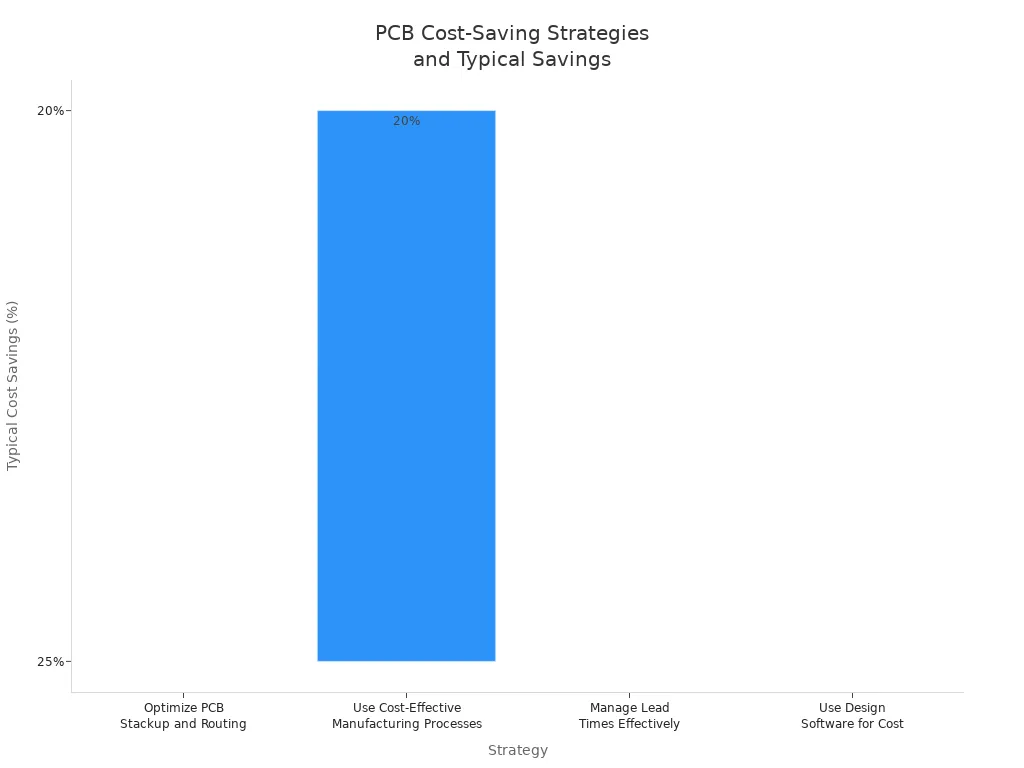
A power supply maker saved 20% per board by switching from ENIG to HASL and making their pcb layout better.
High-Reliability
Devices that must always work need the most reliable pcbs. Engineers pick multilayer, rigid-flex, or ceramic pcbs with strong laminates and gold to stop rust. They use coatings to block water and chemicals. Potting keeps boards safe from pressure and dirt. Vibration mounts and tough connectors keep parts connected in rough places.
Teams check thermal design to keep parts cool.
AOI and X-ray tests make sure solder joints are strong.
Following rules like IPC-6012 Class 3 and MIL-PRF-31032 means high quality.
Using backup parts and lowering stress on parts makes boards last longer.
For example, a satellite company used polyimide multilayer pcbs with coating and vibration mounts for space. Hard tests showed the boards would work well in orbit.
Space-Constrained
Small devices need tiny, packed pcbs. Engineers use multilayer, HDI, flexible, or rigid-flex pcbs to fit more in less space. Special steps like microvias, photolithography, and SMT help make tight layouts and 3D shapes.
Multilayer pcbs with blind and buried vias help fit more traces in small spots.
Flexible pcbs made from polyimide can bend to fit tight places.
Rigid-flex pcbs mix stiff and bendy parts, cutting down on connectors and saving room.
HDI pcbs use microvias and thin lines for tiny devices.
Picking the right material helps with bending, heat, and support.
A phone designer used an HDI pcb with flexible parts to fit lots of features in a slim case. They added more copper for cooling and planned for heat to stop overheating.
Note: Picking the best pcb and way to make it for each job helps devices stay reliable, cool, and safe in all uses.
How to Choose the Right PCB
Assess Priorities
Picking the right PCB starts with knowing what your project needs. Every project is different, so teams should figure out what is most important before making choices.
Key things to think about are:
Project complexity: Check if the design needs special features like multilayer stackups or tiny parts.
Production volume: Decide if you need just a few boards or many.
Performance requirements: See if you need fast signals, good cooling, or strong boards.
Budget constraints: Try to save money but also think about better materials or advanced ways to make the board.
Lead time: Think about how fast you need the board finished.
Quality standards: Look for certifications like ISO 9001 or IPC to make sure the board is always good.
Manufacturer capabilities: Make sure the maker has the right tools and machines for your design.
Technical support: Pick makers who help with design and testing.
Communication: Work with partners who answer quickly and give clear updates.
Tip: Teams should not pick only by lowest price. Good quality, strong boards, and helpful support are better for long-term success.
Consult with Manufacturers
Working with skilled manufacturers helps teams avoid mistakes and make better boards. Makers know a lot and help at every step.
A normal teamwork plan includes:
Talking about the project to set needs, time, and goals.
Checking the design and getting help from engineers, including DFM analysis.
Picking materials and getting advice on special ways to make the board.
Planning assembly with SMT or THT, focusing on quality checks.
Testing and checking to make sure the board is made right.
Final assembly and packing to fit the project.
Delivery and help after making the board.
Makers also use DFA and DFab ideas. They help make layouts easier, use common parts, and pick the best trace widths. These steps lower mistakes, save money, and make boards faster.
Note: Talking to makers early helps get better designs, fewer delays, and stronger boards.
Practical Tips
Experts suggest some easy steps to help pick and make PCBs without problems:
Follow the maker’s DFM rules to stop design mistakes and making issues.
Talk clearly and give correct design files, part lists, and instructions.
Make RFQs with all details, amounts, and times.
Send design files in the right format, like Gerber or ODB++, with full papers.
Pick materials that fit what you need, balancing cost and how well they work.
Work with the maker early to review together and avoid changing designs later.
Use the same board size, hole size, and finish to save money.
Plan stack-up and panel layout for better performance and easy making.
Use automated checks and tests like AOI to make boards better.
Keep good relationships with suppliers and talk often for help.
Make sure boards follow safety and environment rules like RoHS and ISO 14001.
Keep good records and tracking for fixing problems and checking quality.
Pro Tip: Working together early and keeping clear records helps stop delays and makes sure the board is made right.
Picking the right way to make a printed circuit board helps your project do well. Teams need to think about how hard the design is, how much it costs, and how strong it should be.
IPC-2221 rules help make safe layouts, stop mistakes, and get more good boards for any PCB.
Good spacing, putting parts in the right spot, and strong testing save money and make boards better.
Design Concern | Best Practice |
|---|---|
Handling heat | Add thermal vias and put parts in smart places |
Stopping bending | Pick the right lamination and check heat effects with tests |
Talking to skilled makers helps teams not make expensive errors. Looking closely at what the project needs gives strong and good boards.
FAQ
What is the main difference between single-sided and multilayer PCBs?
Single-sided PCBs have just one copper layer. They are used for easy circuits. Multilayer PCBs have many copper layers stacked together. This lets people make more complex designs. Multilayer boards help devices be smaller and work better.
When should engineers choose HDI PCBs?
Engineers pick HDI PCBs when they need fast signals or tiny parts. These boards are best for small, packed layouts. HDI PCBs are used in smartphones, wearables, and new tech devices.
How does surface finish affect PCB quality?
Surface finish keeps copper safe and helps with soldering. ENIG makes a flat, strong surface for tiny parts. HASL is cheaper but may not work well for crowded boards.
Can flexible PCBs replace rigid boards in all applications?
Flexible PCBs can bend and fit into small spaces. They are good for wearables and medical tools. But rigid boards are stronger for big or heavy parts.
Why is early consultation with manufacturers important?
Talking to manufacturers early helps stop mistakes and saves money. Makers give tips on materials, steps, and tests. Working together makes better boards and faster results.
See Also
Choosing The Ideal PCB Prototype Maker For Your Project
Tips For Picking The Best PCB Fabrication Partner
Finding The Perfect PCBA Manufacturer To Suit Your Business