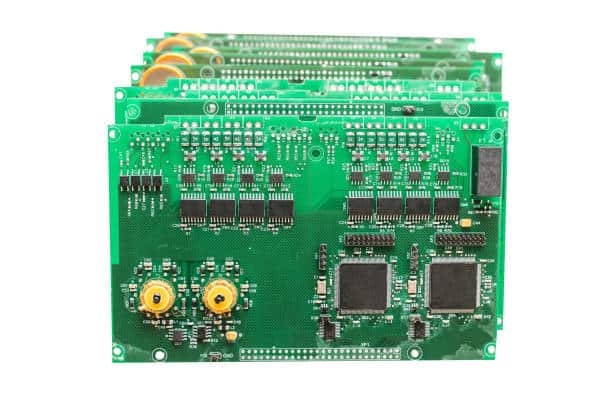
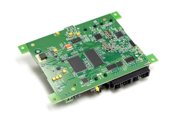
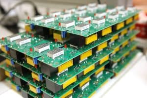
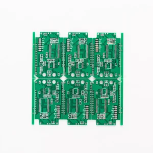
Common Applications of Double-Layer PCBs
✅Industrial Controls (automation, power conversion)
✅Consumer Electronics (audio devices, amplifiers, printers)
✅Mechatronic Equipment (robotics, motor controllers)
✅Automotive Electronics (dashboard controls, LED lighting)
✅Communication Devices (RF applications, networking)
✅Internet of Things (IoT) devices
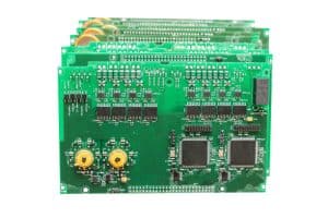
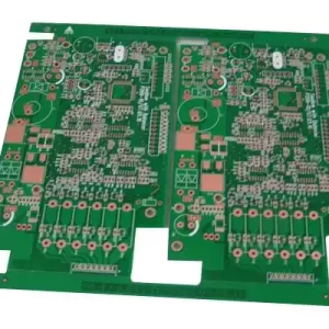
Advantages of Double-Layer PCBs
| Advantage | Description |
|---|---|
| Increased Circuit Density | Enables denser component/trace packing with dual copper layers for complex circuits. |
| Smaller PCB Size | Reduces board size requirements, ideal for compact devices. |
| Better Electrical Performance | Shorter signal paths reduce interference and improve routing efficiency. |
| Enhanced Design Flexibility | Supports intricate designs and multifunctional circuits compared to single-layer PCBs. |
| Cost-Effective | More affordable than multilayer PCBs while offering superior performance to single-layer boards. |
| Plated Through-Holes (Vias) | Enable reliable interlayer electrical connections for improved performance. |
| Stronger & Reliable Connections | Reduces risks of trace breaks and cold solder joints. |
| Wide Applicability | Used in mechatronics, power systems, consumer electronics, and industrial controls. |
| Component Flexibility | Compatible with both through-hole and surface-mount components, enhancing manufacturing efficiency. |
| Improved Heat Dissipation | Better heat distribution than single-layer PCBs, enhancing durability. |
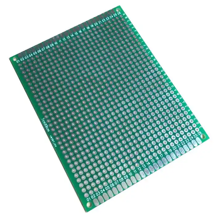
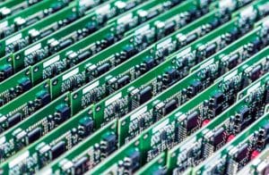
Double-Layer PCBs Manufacturing Process
The Double-Layer PCB manufacturing process is similar to that of Single-Sided PCBs but involves additional steps to create electrical connections between the two copper layers using vias. Below is a step-by-step guide to the process:
1.Design & Layout
The circuit layout is designed using PCB CAD software (e.g., Altium Designer, Eagle, KiCad).
The design includes top and bottom copper layers, as well as via placements for interconnections.
The Gerber files are generated and sent to the PCB manufacturer.
2.Substrate Selection & Preparation
A base material, usually FR4 (fiberglass-reinforced epoxy), CEM-3, or polyimide, is selected.
A copper-clad laminate with copper foils on both sides is prepared.
3.Drilling (Via Hole Creation)
CNC drilling machines create holes for vias, through-hole components, and mounting.
These holes are essential for electrical connections between the top and bottom layers.
4.Hole Plating (Through-Hole Via Formation)
The drilled holes are electroplated with copper to create conductive paths between the top and bottom layers.
This process ensures electrical continuity across the layers.
5.PCB Patterning (Etching Process)
Photoresist Coating: A UV-sensitive film is applied to both sides of the board.
UV Exposure & Development: The circuit design is transferred onto the board using UV light.
Etching: The unprotected copper is etched away, leaving the required conductive traces.
Photoresist Removal: The remaining protective layer is stripped off.
6.Solder Mask Application
A solder mask (usually green) is applied to protect the copper traces from oxidation and solder bridges.
The mask is exposed to UV light and developed, revealing areas for soldering.
7.Silkscreen Printing (Optional)
Component markings, labels, and logos are printed on the PCB for easy assembly.
8.Surface Finishing (Optional)
To improve solderability and corrosion resistance, a surface finish is applied:
HASL (Hot Air Solder Leveling) – Common and cost-effective.
ENIG (Electroless Nickel Immersion Gold) – Used for high-reliability applications.
OSP (Organic Solderability Preservative) – Protects copper without adding thickness.
9.Cutting & Profiling
The PCBs are routed or V-scored into their final dimensions using CNC machines.
10.Electrical Testing & Quality Inspection
Automated Optical Inspection (AOI): Detects any etching defects or misalignments.
Flying Probe or Bed of Nails Testing: Checks electrical conductivity and continuity between layers.
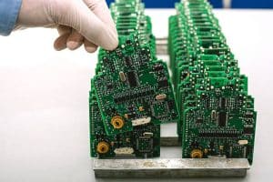
11.Final Cleaning, Packaging & Delivery
The PCBs are cleaned to remove any contaminants.
They are packed according to customer requirements and shipped for PCB assembly (PCBA).
Reviews
There are no reviews yet.