Modern PCB making involves a detailed pcb production process that significantly affects cost and application. Wire bonding uses metals like gold, copper, or aluminum, each with its own cost and unique properties. The extent of machine involvement in the pcb production process greatly influences the overall expense. Choosing the right circuit method is crucial: SMT is ideal for small, densely packed circuits, while THT is better suited for robust, durable circuits. Various techniques in the pcb production process impact the precision and functionality of the board. The materials selected play a vital role as well. Following careful steps throughout the pcb production process ensures high-quality PCBs that meet the specific requirements of the circuit.
Key Takeaways
Picking the right PCB type—rigid, flexible, or HDI—depends on what the device needs. Some devices need more strength. Others need to be small or handle complex tasks. Careful steps like lamination, drilling, plating, and solder masking help make good PCBs. These steps help PCBs last longer and work better. Assembly methods like SMT, THT, and press-fit change how fast the product is made. They also change how strong it is and how easy it is to fix. Testing methods like visual checks, ICT, AOI, and X-ray help find problems early. This makes PCBs more reliable. Automation and green manufacturing help lower mistakes and save money. They also help protect the environment during PCB production.
PCB Manufacturing Methods
Modern electronics need different pcb manufacturing methods to make good circuit boards. Each method has special benefits for certain uses.
Rigid PCB
Rigid pcb manufacturing is the most used in electronics. These boards use hard materials like fiberglass. This gives them strength and helps them last longer. Rigid pcbs are good for devices that need strong support. They also help with heat moving away from parts. You can find them in things like phones, cars, factories, and hospitals. Engineers pick rigid pcbs for circuits that are packed tightly or work at high speeds. These boards do not bend, so they are easy to fix. Multi-layer rigid pcbs can handle tough designs and stop unwanted signals. High-frequency rigid pcbs keep signals clear in wireless and radar systems.
Tip: Rigid pcbs are a good choice when you want something strong and that lasts a long time.
Flexible PCB
Flexible pcb manufacturing uses thin and bendy materials like polyimide. These boards can fit into tiny spaces and let people make cool shapes. Flexible pcbs make devices lighter and smaller. That is why they are used in smartwatches, planes, and the military. They can bend many times without breaking, so they last longer. But, flexible pcbs cost more to make and usually have only a few layers. If you bend them too much, they can break. Fixing them is also harder. Flexible pcbs can get damaged by water or changes in temperature.
Advantages:
Save space and are light
Fit into odd shapes
Limitations:
Cost more to make
Not as strong as rigid pcbs
Additive Manufacturing
Additive manufacturing brings new ways to make pcbs. This method builds boards one layer at a time using 3D printing or inkjet. Designers use CAD software to plan the board. Then, they put down only the needed materials. Additive manufacturing wastes less and makes boards fast, sometimes in just hours. It lets people make tricky shapes and custom boards. But, it can have problems with how well it carries electricity and how neat the lines are. It is best for small amounts or special projects, not for making lots of boards at once.
Manufacturing Method | Description | Key Features |
|---|---|---|
Subtractive Method | Takes away extra copper to make circuit shapes | Old way, used a lot, removes material |
Additive Method | Adds lines by plating or printing | New way, makes thin lines, less waste |
Surface Laminar Circuit (SLC) Technology | Builds layers one by one for blind via making | Faster making, better layer links |
DYCOstrate® Technology | Uses polyimide and plasma etching | Makes thin lines, uses special materials |
PCB Production Process
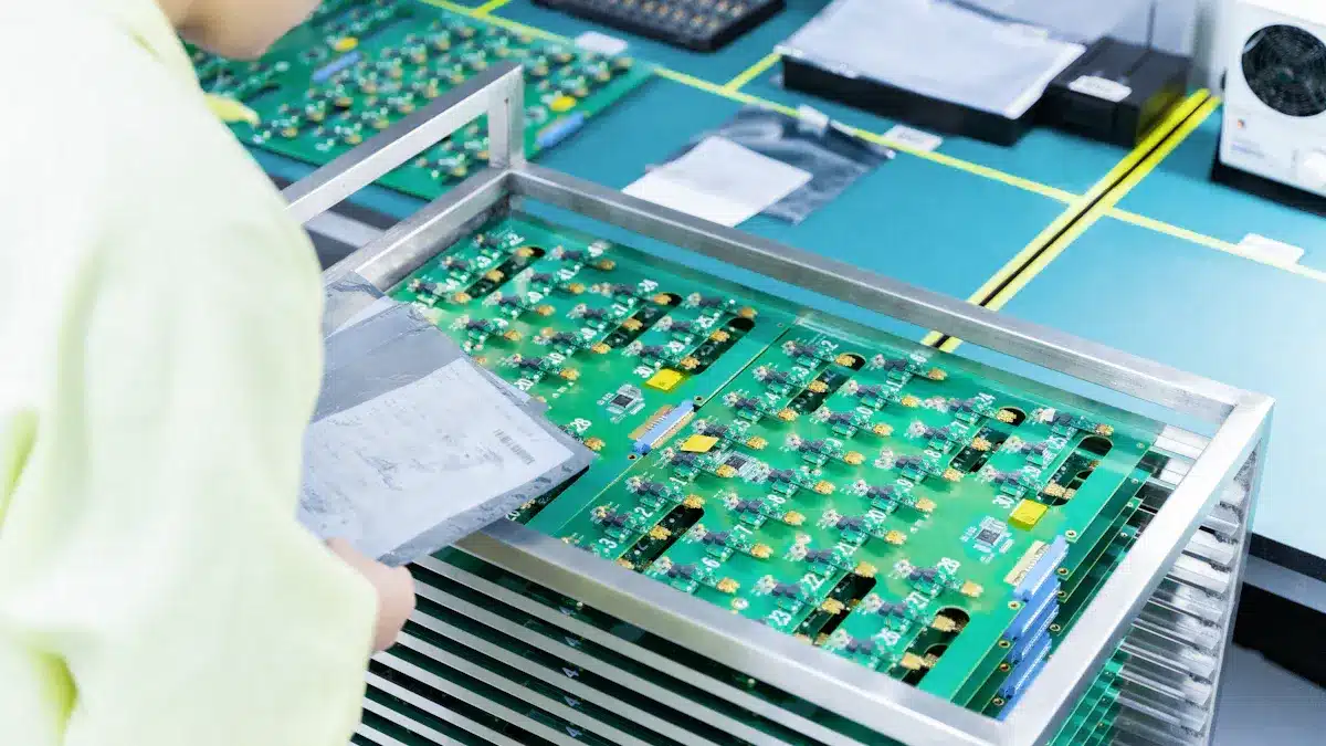
The pcb production process includes several important steps. Each step helps make sure the final pcb works well and lasts a long time. Here is how each stage shapes the circuit and its quality.
Lamination
Lamination joins layers of material together to form a strong base for the pcb. The process uses heat and pressure to bond copper and insulating sheets. This step gives the board its shape and strength. If the lamination is not done right, the board can crack or peel. Good lamination helps the pcb survive stress during later steps in the pcb production process.
Lamination affects stiffness, toughness, and how well the board handles heat.
Small mistakes can cause the circuit to fail or lower the yield.
Drilling
Drilling makes holes for connecting different layers of the pcb. New drilling machines use lasers and sharp bits to make tiny, accurate holes. Laser drilling can make holes as small as 25 microns. This helps with high-density circuits and keeps the pcb production process fast and precise.
Drilled holes must be clean and the right size for good connections.
Real-time checks help catch mistakes early.
Plating
Plating covers the drilled holes and copper traces with a thin metal layer. This step improves electrical flow and protects the circuit from damage. The plating must be even and stick well to the surface. If not, the pcb may have weak spots or lose power over time.
Good plating stops oxidation and keeps the circuit working longer.
Careful cleaning before plating helps the metal stick better.
Etching
Etching removes extra copper, leaving only the needed circuit paths. Most factories use chemical etching, which is fast and cheap but can harm the environment. Plasma etching is cleaner and more precise but costs more. The choice of etching affects how fine the circuit lines can be and the impact on nature.
Solder Mask
The solder mask covers the pcb to protect it from dirt and short circuits. It also keeps solder from spreading during assembly. Liquid photoimageable masks work well for fine lines and high-density boards. The right mask and thickness help the pcb last longer and make assembly easier.
Tip: A good solder mask prevents solder bridges and keeps the circuit safe from moisture.
Surface Finishing
Surface finishing coats the copper pads to stop them from rusting and to help with soldering. Common finishes include HASL, ENIG, and OSP. Each type offers different levels of protection and ease of soldering. The finish chosen depends on the circuit’s needs and cost.
Surface Finish | Solderability | Corrosion Resistance |
|---|---|---|
HASL | Good | Moderate |
ENIG | Excellent | Excellent |
OSP | Good | Limited |
Routing
Routing cuts the pcb into its final shape. Advanced routing lets designers fit more parts in less space. This step is key for making small, complex circuits. Good routing helps the pcb fit into its case and work with other parts.
The pcb production process uses careful steps to make sure each circuit meets high standards. Quality checks at every stage help catch problems early and keep the final product reliable.
PCB Manufacturing Techniques
HDI
High-density interconnect is a very advanced way to make pcbs. HDI pcbs use microvias and special vias to fit more parts in less space. They also have very thin lines. This lets engineers make small and complex boards with many layers. HDI helps build devices that are smaller, lighter, and faster. Shorter traces in HDI boards help signals stay clear and reduce noise. That is why HDI is used in phones, medical tools, and cars.
Feature | Description |
|---|---|
Microvias and fine lines | Help make tiny, complex connections |
Multiple copper layers | Allow for more parts and tricky designs |
Ultra-thin cores | Make boards smaller and lighter |
As little as 0.075mm for tiny circuits |
Note: HDI pcb manufacturing techniques help save power and make electronics work better.
Impedance Control
Impedance control is important for making fast electronic pcbs. Engineers plan the width and space of traces to keep impedance steady. This stops signals from bouncing back and causing mistakes. Using materials like FR4 helps keep impedance the same. Special tests check if the pcb meets the right values. Impedance control is needed for hard designs in telecom, computers, and cars. It helps signals stay strong and data move safely.
Controlled impedance stops signals from mixing and keeps timing right.
Using pairs and good ends helps signals stay steady.
Blind and Micro Vias
Blind and micro vias are tiny holes that connect layers without going through the whole board. These help fit more connections in a small space. This is good for boards with lots of parts and tricky designs. Blind vias can make pcbs up to 30% smaller. Micro vias make signals better by making paths shorter and cutting down signal loss. But, they need careful filling and plating to work well. Staggered micro vias last longer than stacked ones.
Benefits:
More parts in less space and smaller boards
Better signals and faster data
Challenges:
Harder to make and cost more
Need careful drilling and plating
Back Drilling
Back drilling is a way to take out extra parts of vias called stubs. Stubs can make signals bounce and cause noise. Removing them keeps impedance steady and cuts down signal loss. Back drilling is used for fast and complex boards like 5G, radar, and data centers. It helps these boards handle fast data and keeps signals clear.
Takes away via stubs to stop signal bounce
Cuts down on signal mixing and noise
Works for speeds over 10 GHz in new tech
PCB Assembly Process
The pcb assembly process puts all the parts together. Each way to assemble has its own steps and tools. Picking the right way helps the pcb work well and last longer.
SMT
Surface mount technology changes how we build electronics. Tiny parts go right on top of the pcb. Machines do most of the work, so it is fast and correct. Special paste and ovens help stick the parts on. This way, more parts fit in a small space. Devices can be smaller and lighter.
Aspect | SMT (Surface Mount Technology) | THT (Through-Hole Technology) |
|---|---|---|
Machines place parts quickly and cut down time. | People do more work, so it is slower and mistakes can happen. | |
Reliability | Small parts make it steady and less heat hurts it, but it is not as strong if you shake it. | Not as steady, but good for big power and when things get hot or move a lot. |
Additional Notes | Uses solder that is better for the planet. Machines help make every board the same. | Solder can make bad smoke. It is better at moving heat away but can break from heat. |
Surface mounting is fast and works well. It also uses safer solder for the earth. Many companies use it for phones, computers, and medical tools.
Tip: Surface mount technology is best for small, tricky circuits that need quick, machine assembly.
THT
Through-hole technology does things differently. People or machines put parts with long wires into holes. Solder keeps the parts in place. This takes longer and needs skilled people. The connections are strong and handle heat and shaking.
THT is good for big parts and strong circuits. It helps when the pcb will shake or get bumped. Power supplies and car parts often use THT because it is tough.
Press-Fit
Press-fit assembly skips solder and uses tight holes. Parts are pushed in and stay because they fit tightly. No heat is needed, so parts do not get hurt. Press-fit can handle shaking and bumps better than solder. It is also easier to fix. You can take out and put in parts without breaking the pcb.
Aspect | Press-Fit Assembly | Soldered Connections |
|---|---|---|
Stays strong when things shake or get hit; good for rough places. | Can break more easily if things shake or get hit. | |
Thermal Impact | No heat, so nothing gets burned. | Needs heat, which can hurt parts or the board. |
Ease of Repair | Easy to take out and put in parts without harm. | Fixing needs heat and can break the board. |
Easier for machines and does not need special skills. | Needs skilled people and special tools like irons and ovens. |
Press-fit keeps parts safe from heat and makes fixing easy. Car and phone companies use press-fit for hard jobs.
Note: Press-fit assembly saves time and money. It makes repairs easy and stops heat from hurting the board.
Material Selection
Processing Ease
Picking the right material makes the pcb easier to work with. Some materials are easy to cut and drill. Others need special tools or extra care. Here are some common materials:
FR-4: This is the most used rigid pcb material. It has fiberglass and epoxy resin. FR-4 is simple to use for many jobs.
Polyimide laminates: These are flexible and can bend without breaking. They handle heat well but need careful handling.
Teflon (PTFE): This material is great for electricity. It is hard to cut and drill, so it costs more.
Composite epoxy materials (CEM): These can take high heat and are good for crowded boards.
Flexible laminates: Materials like polyester and liquid crystal polymer can bend and fold. They need gentle handling to keep their shape.
PCB Material | Dielectric Constant | Dissipation Factor | Thermal Conductivity | Flexural Strength | Glass Transition Temp |
|---|---|---|---|---|---|
FR-4 | ~4.5 | ~0.02 | 0.3 | 400-800 MPa | 130-180°C |
Polyimide | 3.2-3.6 | 0.002 | 0.2 | 200-400 MPa | 260-400°C |
PTFE | 2.1 | 0.0002 | 0.25 | 10-20 MPa | N/A |
Tip: FR-4 is a smart pick for most projects. It is strong, not too expensive, and easy to work with.
Suitability
Suitability means picking the best material for the job. Each use needs certain things for the pcb to work well. For example, high-frequency circuits need materials like PTFE. Devices that bend, like wearables, use flexible laminates such as polyimide or polyester. Rigid-flex pcbs mix rigid and flexible parts for tricky devices like smartphones.
Engineers also check how well a material handles heat, water, and stress. Metal core pcbs are good for LED lights because they move heat away. Materials with high glass transition temperatures can take the heat from soldering. Good material choice helps the pcb last longer and keeps signals clear.
FR-4: Good for most uses and balanced performance.
Polyimide: Great for flexible circuits and hot places.
PTFE: Used for fast or radio frequency boards.
CEM: Picked for crowded and hot boards.
Metal core: Used when moving heat is most important.
Note: Picking the right material helps the pcb work well and last longer.
Testing Methods
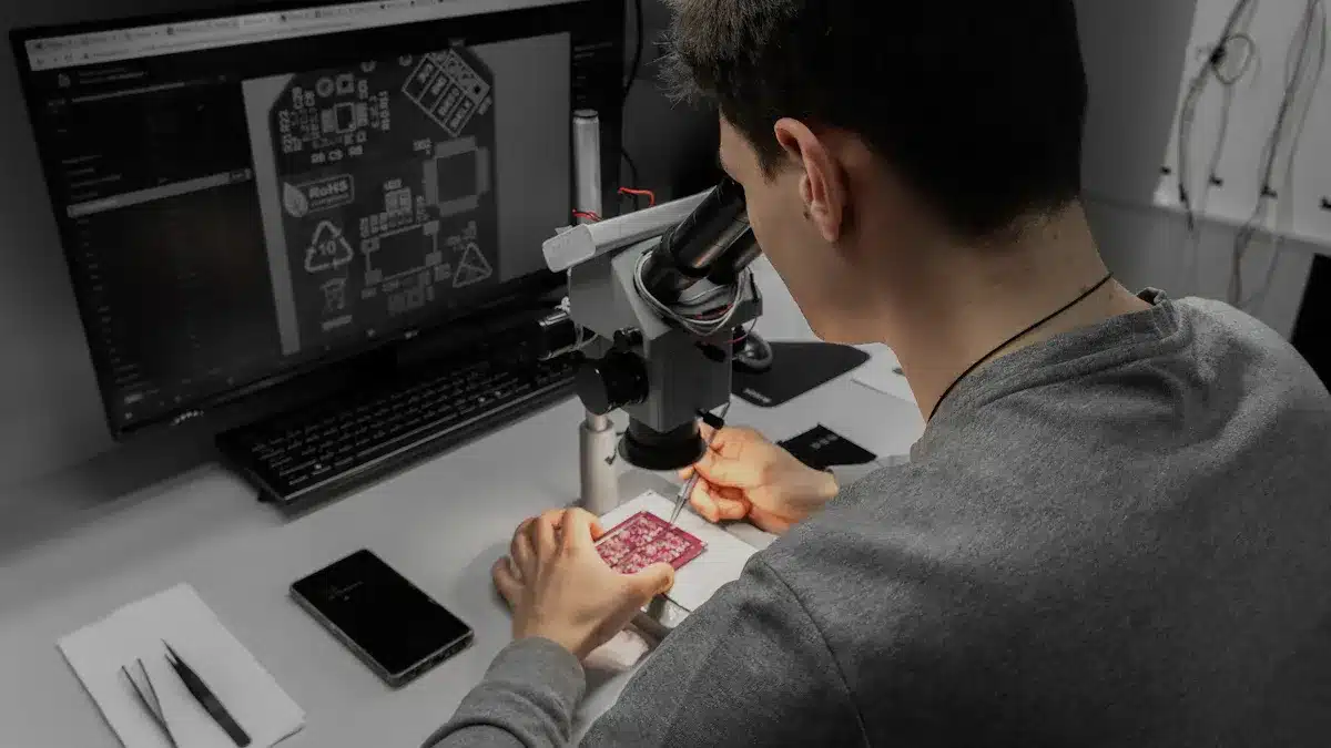
PCB makers use different ways to test every board. These tests help find problems early. They also make quality control inspections better. Each test looks for certain mistakes. Some tests work best in special cases.
Visual Inspection
Visual inspection is the first check in quality control inspections. People or machines look for things like missing parts or bad solder joints. They also check if parts are in the wrong place. This test is cheap and simple to do. It finds big problems fast. But it cannot see problems under parts or inside the board. People can also make mistakes when checking.
In-Circuit Testing
In-circuit testing, or ICT, uses special probes to test each part. ICT turns on the board and checks for shorts and broken parts. It finds problems that visual inspection misses, like lifted pins. ICT works quickly and finds up to 98% of problems in big batches. It helps quality control inspections by finding issues early and saving money.
ICT can test hundreds of parts in just seconds. It finds problems even in boards with tiny parts.
Flying Probe
Flying probe testing uses moving probes to touch many spots on the board. It does not need a special fixture, so it is good for new designs and small groups. Flying probe checks for shorts and other electrical problems. Sometimes it covers more than ICT, but it is slower. It cannot find some solder problems.
AOI
Automated optical inspection, or AOI, uses cameras to take pictures of the board. AOI compares these pictures to a model and finds differences. It spots surface problems like parts in the wrong place or solder bridges. AOI is fast and helps find problems early. But it cannot see under parts.
X-ray
X-ray inspection looks inside the board without opening it. It finds hidden problems like solder voids and bridges under chips. X-ray can see very small problems, even 25 microns wide. New 3D X-ray scans check many layers and find more mistakes. This test is important for boards used in planes and hospitals.
X-ray inspection finds up to 98% of hidden solder problems. It is very important for tricky boards.
Burn-In
Burn-in testing runs the board hot and with lots of power for a long time. This test finds early failures and hidden problems. Burn-in makes boards more reliable but takes a lot of time. It can also make the board not last as long.
Functional Testing
Functional testing checks if the board works like it should. It acts like real use and tests all the features. How well it works depends on the test plan. This test is flexible and costs less than special tests. It might miss early problems if the test is not complete.
Testing Method | Key Features | Detection Rate / Coverage | Notes |
|---|---|---|---|
Visual Inspection | Manual check for visible defects | Basic defect detection | Cheap, easy, limited to visible joints |
In-Circuit Testing (ICT) | Powers and tests each part, high coverage | Fast, best for large volumes, needs test fixture | |
Flying Probe Testing | Automated probes, flexible for prototypes | Higher coverage than ICT in some aspects | No fixture needed, slower, not for mass production |
AOI | Cameras compare images to templates, flags surface defects | Good for early defect detection | Fast, only surface defects detected |
X-ray | Internal imaging, finds hidden defects | Highest detection rates | Expensive, skilled operators needed |
Burn-In | Stress test under extreme conditions | Very effective for latent defects | Time-consuming, may reduce lifespan |
Functional Testing | Simulates real use, checks all functions | Depends on test plan | Flexible, customizable, may miss early failures |
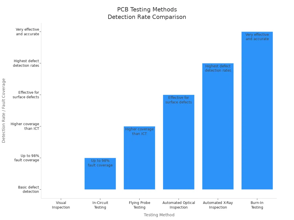
Testing and prototyping help engineers pick the best test for their project. Each test makes boards better and lowers the chance of problems in the end.
Summary
Cost
The price to make PCBs depends on how many you make, what materials you use, and which process you pick. Making just a few prototype boards costs the most for each one. This is because people do more work by hand and there are setup fees. When you make more boards, machines help and the cost for each board goes down. This happens because making lots at once saves money. What you pick for materials, surface finish, and testing also changes the final price.
Quantity Range | Tooling Costs | Production Process | Cost per Board | |
|---|---|---|---|---|
Prototype | 1-5 units | Minimal | Manual | Very High |
Low Volume | 10-100 units | Moderate | Automated | Moderate |
High Volume | 1000+ units | High | Automated | Low |
Production Volume Range | Approximate Unit Cost (USD) | Explanation |
|---|---|---|
$50 – $200 | High fixed costs lead to very high unit costs. | |
10-100 units | $20 – $100 | Costs begin to dilute with volume increase. |
100-1000 units | $10 – $50 | Economies of scale start to reduce costs. |
1000-10000 units | $5 – $30 | Significant unit cost reduction. |
10000+ units | $2 – $20 | Fixed costs fully diluted, lowest unit cost. |
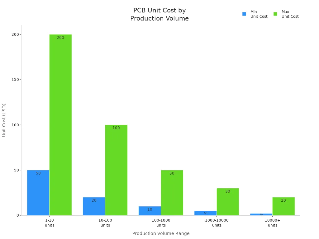
Tip: Making lots of boards at once saves money. Small batches and prototypes cost much more for each board.
Precision
Modern PCB factories can make very tiny and exact parts, especially with new machines. Regular drilling makes holes as small as 0.2 mm. Laser drilling can make even smaller holes, down to 0.1 mm or less. Smaller holes help signals but cost more and need special makers.
Mechanical Drilling | Laser Drilling | |
|---|---|---|
Minimum Drill Size | ~0.2 mm | ≤0.1 mm |
Aspect Ratio Limit | Up to 10:1 | 10:1 or better |
Cost Impact | 10-20% higher for smaller holes | Even higher due to equipment |
Manufacturer Capability | Most support ≥0.2 mm | Only specialized support ≤0.1 mm |
Signal Integrity | Good | Excellent |
1. Most companies offer regular tolerances for less money. 2. Tighter tolerances need better tools and cost more. 3. High aspect ratios can cause more problems. 4. Not all companies can make very tiny holes. 5. Important holes need extra care for best results.
Note: Laser drilling lets you make smaller features but costs more and not all companies can do it.
Complexity
PCBs get more complicated when they are smaller, have more layers, or use new features. HDI boards use microvias and thin lines, which makes them harder to build. Flexible and rigid-flex boards need special materials and careful work. High-speed boards need exact impedance control and special materials.
Description | |
|---|---|
Multi-layer PCBs | Need careful lining up and drilling, which is harder and costs more. |
HDI PCBs | Use microvias and thin lines, so they need skilled workers and good machines. |
Flexible PCBs | Need special materials to stay bendy and conduct electricity. |
Rigid-Flex PCBs | Mix stiff and bendy parts, which makes design and building tricky. |
High-Speed PCBs | Need exact impedance control to keep signals clear. |
Miniaturization | Uses thin layers and hidden parts, which adds to the challenge. |
Thinner boards and more layers make building harder.
Hidden parts help performance but make design tougher.
New green rules and standards mean factories must change fast.
Tip: Harder boards need smart engineers and good machines.
Automation
Automation helps PCB factories work faster and make better boards. Machines put parts in the right place with great accuracy. This means fewer mistakes and less waste. Automated checks find problems early and fix them right away. Robots and smart systems make work flexible and help keep machines running.
Machines can work all the time, so more boards get made.
Fewer errors happen because machines follow exact steps.
Quality checks catch problems and lower the number of bad boards.
Robots can handle very small parts well.
It costs a lot to start, but you save money over time.
A study showed that after using automated checks, defects dropped from 0.9% to 0.14%. Lot rejection went down from 5500 PPM to 900 PPM. This proves automation makes things better and faster.
Note: Automation makes PCB making quicker, safer, and more dependable.
Environmental Impact
Making PCBs can hurt the environment because of the materials, chemicals, and waste. Old ways of etching use chemicals that can pollute. Additive manufacturing and plasma etching make less waste and are cleaner. Lead-free solder and green materials help lower toxic stuff. Automation also cuts waste by being more exact and making fewer mistakes.
Method/Technology | Environmental Impact |
|---|---|
Subtractive Etching | High chemical waste |
Additive Manufacturing | Low waste, cleaner process |
Lead-Free Solder | Less toxic emissions |
Automation | Less material waste |
Green Materials | Lower pollution, safer |
Factories now use safer chemicals and recycle more.
Green rules make companies use eco-friendly ways.
Automated systems help watch and cut down waste.
Tip: Picking green materials and clean processes helps the earth and follows new rules.
Selection Guide
Project Needs
Each project needs something different. Engineers must think about what the circuit does. They also look at where people will use it. Some projects need boards that bend. Other projects need boards that stay strong for a long time. Flexible PCBs are good for small and light devices. Rigid PCBs are best for strong support. If there are lots of tiny parts, surface mount technology saves space. It also makes building faster.
People should ask these questions before they start:
What size and shape does the board need?
Will the board get hot, wet, or shake?
Does the project need fast signals or lots of power?
How many boards will the team make?
Will the board need easy fixing or upgrades?
Surface mount technology is good for phones and computers. It also works for medical devices. Through-hole assembly is better for power supplies and car parts. Press-fit assembly helps when repairs must be quick and easy.
Tip: Engineers should pick the PCB type and assembly method that match the project’s main goals.
Decision Factors
Picking the right PCB method means looking at important things. Each thing changes how the board works and how much it costs.
Factor | Why It Matters | Example Projects |
|---|---|---|
Application | Some boards need to bend, others must stay rigid | Wearables, industrial machines |
Budget | More layers and special materials cost more | Prototypes, mass production |
Design Complexity | Complex designs need advanced tools and methods | Smartphones, radar systems |
Volume | Large batches lower the cost per board | Consumer electronics |
Surface mount technology speeds up assembly | Tablets, smartwatches | |
Repair Needs | Press-fit assembly makes fixing easier | Automotive, telecom |
Engineers must plan so factories can build the board easily. Hard designs often need surface mount technology. They may also need special steps to put together. If a project needs high speed or tiny parts, HDI and impedance control are important. Flexible boards need careful picking of materials and assembly.
Surface mount technology helps with fast building and small parts. Through-hole assembly is good for strong connections. Press-fit assembly saves time and makes fixing easy.
PCB manufacturing methods use different materials and steps. They also have different ways to put boards together. Engineers pick the assembly type that fits what the project needs. Some projects need strong boards, while others need flexible ones. The way you put the board together changes how much it costs. It also changes how fast you can make it and how easy it is to fix. Teams should think about what they need before they start designing. Experts say to match the assembly method to where and how the device will be used. If a project is tricky, engineers often ask specialists for help.
Tip: Planning each assembly step carefully helps you get better boards and make fewer mistakes.
FAQ
What is the main difference between rigid and flexible PCBs?
Rigid PCBs are made from hard stuff like fiberglass. Flexible PCBs use soft materials such as polyimide. Rigid boards do not bend and stay strong. Flexible boards can twist and fit into tight spots.
Why do engineers choose HDI technology?
Engineers use HDI technology to add more parts to small boards. HDI has tiny holes and very thin lines. This makes devices lighter and work faster. Phones and medical tools often need HDI.
How does automation improve PCB manufacturing?
Automation means machines put on parts and check for mistakes. This helps make fewer errors and builds boards faster. Factories can make more boards in less time. Machines also help cut down on waste.
Which PCB testing method finds hidden defects best?
X-ray inspection looks inside the board for hidden problems. It checks for solder issues under chips and between layers. Engineers use X-ray for tricky boards in medical and airplane devices.
See Also
Emerging Innovations Shaping PCB And PCBA Design Processes
Benefits And Obstacles Of Flex PCBA In Electronics
In-Depth Look At PCBA Testing Methods For Electronics
Best Practices To Boost Quality And Efficiency In PCBA
The Importance Of Custom PCBA Manufacturing In Today’s Electronics
