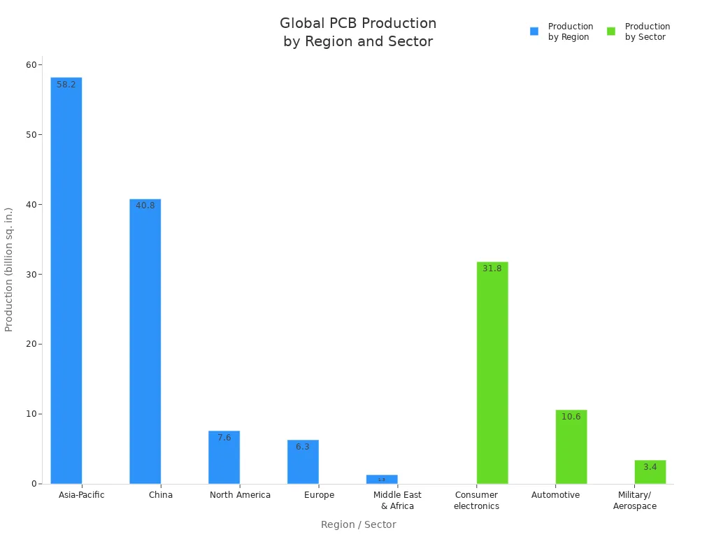
A printed circuit board (PCB) is a flat base that does not conduct electricity. It has thin lines that do conduct electricity. These lines connect electronic parts together. Engineers use PCBs to hold and link parts inside devices. When people ask what is printed circuit board, they mean this important part. PCBs help power over 19.3 billion connected devices around the world. The table below shows how many PCBs are made each year.
Aspect | Data / Description |
|---|---|
Total global PCB production | |
Number of electronic components mounted | More than 2.1 trillion components mounted on PCBs |
Number of connected devices powered | Over 19.3 billion connected devices worldwide |

PCBs are the main part of modern electronics. If you want to know what is printed circuit board, you should know this. PCBs help make fast connections in things like phones and cars.
Key Takeaways
Printed circuit boards (PCBs) link and support electronic parts with copper lines. This helps devices become smaller, work faster, and be more dependable.
PCBs have layers and parts that manage power, heat, and signals. This lets engineers make electronics that work better and last longer.
There are many PCB types for different uses. Some are simple with one layer. Others are complex with many layers for phones, computers, and smart gadgets.
What Is Printed Circuit Board?

Printed Circuit Board Definition
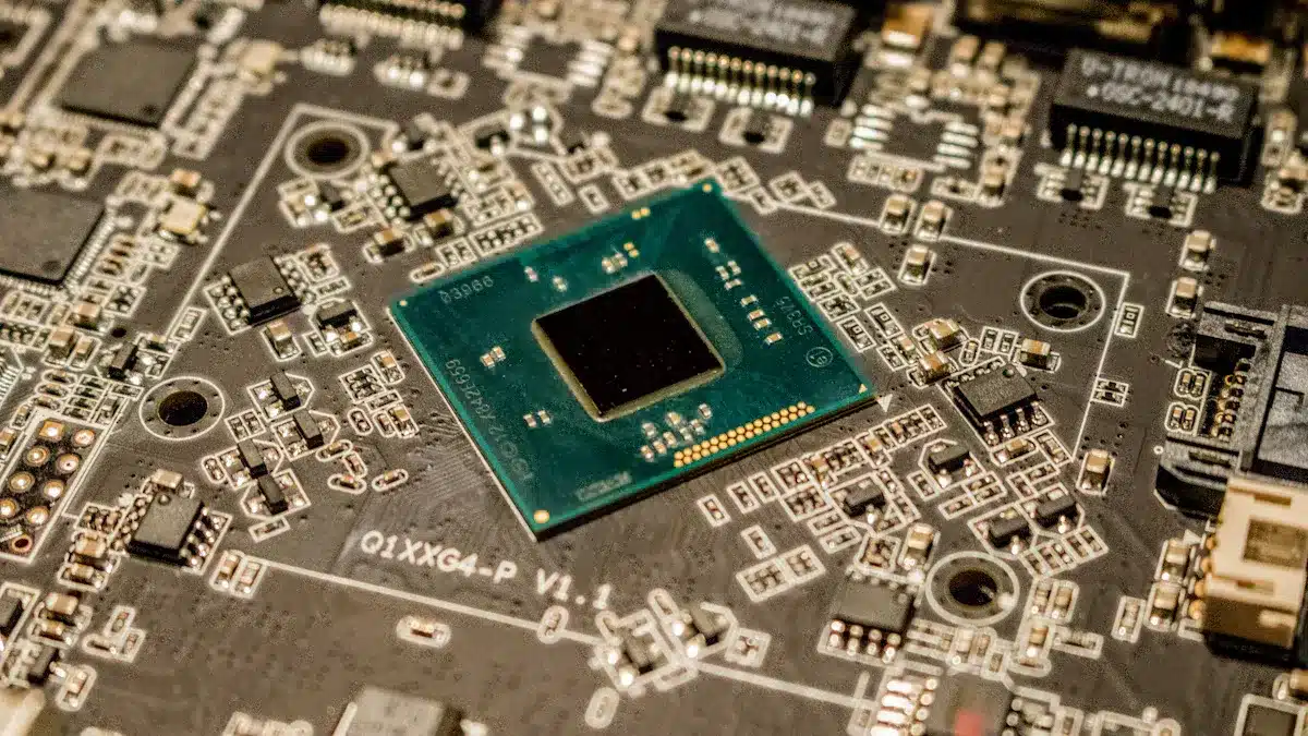
A printed circuit board, or PCB, is a flat board. It connects and holds electronic parts. Some people call it a “printed wiring board” or just “board.” The main job of a PCB is to keep parts and their links together. Most PCBs use a strong base like fiberglass. Some use flexible or mixed materials. Engineers put parts like diodes and transistors on the board. Thin copper lines called traces connect these parts. Traces let electricity move between them. This setup matches what big electronics groups say. When someone asks about a printed circuit board, they want to know about this important base. It helps electronic devices work.
Note: People in electronics often say “printed wiring board.” They may also call it a “board.”
PCB Function in Electronics
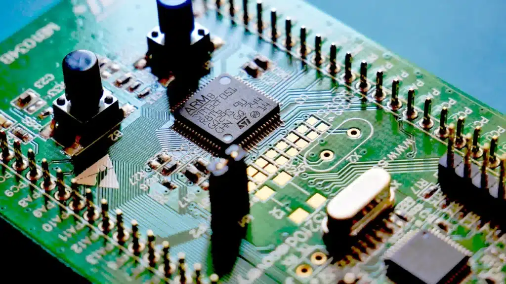
A PCB is the backbone of most electronics. It holds and links all the parts a device needs. The board uses special features to do its job:
Traces are thin copper lines that link parts.
Pads are small metal spots for soldering parts.
Vias are tiny holes for signals to move between layers.
Silkscreen has printed labels to show where parts go.
Designing a PCB means planning where each part goes. It also means choosing how to route the traces. Good design helps devices work better and last longer. Engineers attach parts in two main ways. Through-hole mounting puts part leads through holes and solders them. Surface mount technology puts parts right on the board’s surface.
PCB Feature | Purpose |
|---|---|
Substrate | Supports parts and stops electricity from leaking |
Copper traces | Carry signals and power between parts |
Solder mask | Protects copper traces from damage and shorts |
Silkscreen | Shows labels and symbols for placing parts |
People ask what a printed circuit board does. The answer is simple. PCBs connect many parts in a small space. They use neat traces instead of messy wires. This makes devices smaller and lighter. It also makes them more reliable. PCBs help companies make lots of devices fast and cheap.
PCBs are key in modern electronics. They support and connect parts in phones and cars. The design of a PCB affects how well a device works. Good design helps control power and heat. It keeps signals clear. Engineers use PCB design to fit more parts in less space. This makes devices stronger and smaller. Good design also stops problems like short circuits.
PCBs matter because they:
Give a strong base for all parts.
Make connections with copper traces, not wires.
Help build products quickly and easily.
Let devices get smaller and smarter.
Make devices more reliable by stopping wiring mistakes.
If you want to know what a printed circuit board is, remember this. PCBs help electronics be small, fast, and reliable. Every step in design, from picking materials to planning the layout, makes better devices. Circuit board design helps new technology grow.
Printed Circuit Board Structure

Printed Circuit Board Layers
A printed circuit board is made like a sandwich. It has layers of copper and layers that do not conduct electricity, like fiberglass or resin-bonded paper. Each layer has its own job in pcb design. The main printed circuit board layers are:
Signal layers move electrical signals between parts.
Plane layers give power and ground, and help stop noise.
Prepreg layers stick copper sheets together and add insulation.
Internal layers are often used for power or ground.
External layers have copper traces and pads for parts.
Solder mask layers keep copper safe and stop short circuits.
Silkscreen layers show text and symbols to help with assembly.
When you add more layers to a pcb, it helps stop noise and keeps signals clear. Multi-layer boards let you make smaller boards and help control heat. These things help advanced electronics work well.
Printed Circuit Board Components
Engineers put many kinds of parts on a pcb. Passive parts like resistors, capacitors, and inductors store or control energy. Active parts like diodes, transistors, and integrated circuits change and boost signals. Other printed circuit board parts are fuses, switches, relays, sensors, and crystal oscillators. Traces are paths for electricity, pads are spots to solder, and vias link layers together. All these things make a strong network for signals and power. Good pcb design puts parts in smart places for easy building and good performance.
Tip: Placing parts carefully and planning trace paths helps make assembly easier and devices more reliable.
PCB Materials
Most pcbs use FR-4 for the base. FR-4 is made from fiberglass and epoxy resin. It is strong, keeps electricity inside, and does not burn easily. Some boards use polyimide to bend or aluminum to handle heat better. Copper is used for traces and planes because it carries electricity well, does not get too hot, and sticks to the base. Solder mask and silkscreen layers use special plastics and inks to protect and label the board. Resin-bonded paper is cheaper but not as strong or heat-proof as fiberglass. Engineers pick materials based on what the pcb and final product need.
PCB Types and Applications
Common PCB Types
Printed circuit boards have different main types. Each type helps with different needs in design and building. The single-layer pcb is the most basic type. It has traces and parts on one side only. This simple type is good for cheap and easy devices.
Double-layer pcb designs have two layers. Engineers put traces and parts on both sides. Through-hole vias link the two layers together. This lets the board hold more parts and have more paths.
Multilayer pcb designs use three or more layers. Prepreg keeps each layer apart. Vias connect the inside layers. These boards help with advanced paths and power. Multilayer pcbs are used in computers and big machines.
PCB Type | Layers | Structure Description | Key Differences |
|---|---|---|---|
Single-sided PCB | 1 | Conductive traces and components on only one side of a non-conductive substrate. | Simplest structure, low cost, limited routing options, used in simple devices. |
Double-sided PCB | 2 | Conductive traces and components on both sides connected by through-hole vias. | More complex routing, higher component density, better signal integrity. |
Multi-layer PCB | 3 or more | Multiple conductive layers separated by insulating prepreg, laminated together with vias. | Highest complexity and density; advanced routing; used in high-performance systems. |
Other types include flexible pcbs made from thin stuff. These boards can bend and twist for things you wear. Rigid-flex pcbs mix stiff and bendy parts for small builds. High-density interconnect pcbs use tiny traces and holes for small gadgets.
Tip: Picking the right pcb type helps engineers match what the device needs.
PCB Applications
PCBs are important in many electronic products. Rigid pcbs are used in laptops, phones, and game consoles. Flexible pcbs are found in foldable phones and smart screens. Rigid-flex pcbs help with tricky designs in cameras and fancy phones.
Factories use multilayer pcb and HDI boards. These boards run machines, sensors, and building controls. Engineers use them for motors, cameras, and smart home gear. Computers use multilayer pcb for heat and hard circuits.
Audio devices like music players and recorders
Video devices such as cameras and video recorders
Storage devices like hard drives and USB sticks
Smart lights for homes
Power converters and supply devices
Kitchen tools like fridges and ovens
Video game consoles
Security cameras and alarm systems
Laptops and PCs
Computer extras like mouse and keyboard
Office tools such as printers and scanners
PCBs also help sensors in factories and smart gadgets. These sensors check temperature, pressure, and shaking. More smart gadgets and IoT tech need smaller and lighter pcb designs. Engineers work on pcb design to make power, heat, and safety better.
Note: The pcb market keeps growing as smart gadgets and IoT get bigger. Better pcb design helps new electronics work well.
Printed circuit boards hold electronic parts and link them with copper traces.
They help make devices smaller and easier to put together. They also make devices work better and break less often.
If engineers know about PCB layers and parts, they can design better electronics.
PCBs help phones, cars, and smart gadgets work safely and last a long time.
PCBs are very important for today’s technology.
FAQ
What does a PCB look like?
A PCB looks like a thin, flat board with green or blue coating. Copper lines and small metal spots cover the surface.
Tip: Most PCBs have printed labels to help with assembly.
Why do engineers use PCBs instead of wires?
Engineers use PCBs because they make devices smaller, faster, and more reliable. PCBs help connect many parts neatly without messy wires.
Devices last longer.
Can a PCB break or stop working?
Yes, a PCB can break if it gets too hot or damaged. Water, dust, or strong impacts may cause problems with the board.
Problem | Cause | Result |
|---|---|---|
Overheating | Too much heat | Board failure |
Physical shock | Dropping device | Broken traces |
Moisture | Water exposure | Short circuits |
See Also
The Impact Of PCBA On Advancing Modern Electronics
The Importance Of Custom PCBA Production In Electronics
Benefits And Obstacles Of Flex PCBA In Electronics
What PCBA Means And Its Function In Electronics
Exploring PCBA Meaning And Its Essential Uses In Electronics
