
Modern robotic sensors utilize miniaturized PCBs for robotic sensors to operate effectively in confined spaces. These miniaturized PCBs incorporate advanced features within compact designs, making them ideal for powerful systems. A miniaturized PCB for robotic sensors not only conserves space but also performs reliably under challenging conditions. Engineers meticulously design these miniaturized PCBs to achieve an optimal balance of size, strength, and functionality. By managing demanding tasks in limited areas, miniaturized PCBs for robotic sensors are revolutionizing the performance of robotic systems.
Key Takeaways
Small PCBs save space and help robotic sensors work better. They are very important for modern robots.
New methods like HDI and layered designs make PCBs smaller and stronger. This helps them fit and work well in small areas.
Good power use is important for small PCBs. It keeps robotic sensors working longer by stopping heat and energy waste.
Engineers and designers must work together to make good small PCBs. This makes sure they meet both technical and practical needs.
New ideas like bendable PCBs and 3D circuits are changing small PCB designs. These make them work better and help the environment.
Miniaturized PCBs for Robotic Sensors
What Are Miniaturized PCBs?
Miniaturized PCBs are small circuit boards that fit tight spaces. They are important for modern gadgets, especially robots with limited room. Unlike regular PCBs, these focus on being smaller but still powerful. Engineers use special methods like HDI and multilayer designs to make them.
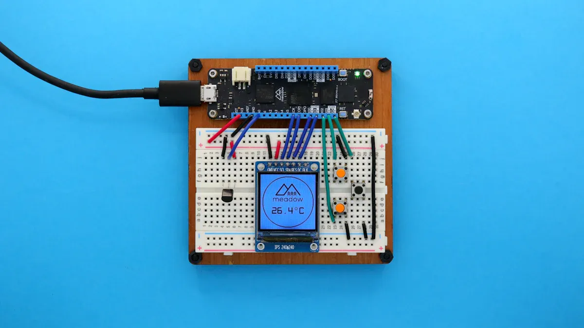
In robotic sensors, mini PCBs are very important. For instance, a proximity sensor uses them to handle signals quickly. Their small size helps them fit into places like robot arms or drones. This technology has become a key part of today’s robotics.
Importance of Miniaturized PCBs in Robotics
Mini PCBs are crucial in robotics because they combine many parts into one system. This helps robots do harder tasks better. For example, a proximity sensor for avoiding obstacles needs a good mini PCB for fast and accurate work.
The need for mini PCBs is growing fast. Reports show the market will grow from $1.2 billion in 2024 to $2.5 billion by 2033. That’s a yearly growth of 9.5%. This shows how much robotics depends on smaller circuit boards.
Benefits of Miniaturization for Robotic Sensors
Making PCBs smaller has many advantages for robotic sensors. First, it makes robots lighter and easier to move. Second, it improves how well sensors, like proximity sensors, work. Third, it cuts costs by using fewer materials and better methods.
Mini PCBs also allow advanced features. For example, flexible mini PCBs in touch sensors let robots feel pressure. Proximity sensors also work better with improved PCB layouts. These upgrades make mini PCBs a must-have for modern robots.
Technologies Behind Smaller PCBs
High-Density Interconnect (HDI) Technology
HDI technology helps make PCBs smaller and more powerful. It uses tiny holes, thin lines, and light materials to fit more parts in less space. Think of HDI as the key to modern gadgets like phones and robotic sensors. It lets them do more without getting bigger.
One big benefit of HDI is simplifying designs. For example, research by Happy Holden shows HDI can turn an 18-layer PCB into just 8 layers. This saves money and boosts performance. That’s why HDI is perfect for robotic sensors, where space and efficiency matter most.
HDI also improves signals by keeping parts closer together. This reduces signal loss and makes the system work better. Whether it’s a touch sensor or a proximity sensor, HDI ensures the PCB works well even in tough conditions.
Multilayer and Rigid-Flex PCB Designs
Multilayer and rigid-flex PCBs are great for small and smart robots. Multilayer PCBs stack circuits to save space while adding features. Rigid-flex PCBs mix stiff and bendable materials, making them strong and flexible.
These designs are ideal for robots. For example, rigid-flex PCBs connect parts in robot arms for smooth communication. They also help fit PCBs into tight spots. Standards like IPC-6013 and IPC-2223 ensure these designs handle heat and bending, keeping them reliable.
Rigid-flex PCBs also make production easier by combining parts into one unit. This lowers the chance of problems and speeds up manufacturing. Whether for factory robots or medical robots, these designs offer the strength and flexibility needed.
Standard | Purpose |
|---|---|
IPC-6013 | Tests heat and bending durability. |
IPC-2223 | Ensures smooth use in mixed systems. |
Advanced IC Packaging and Flexible Substrates
Advanced IC packaging and flexible materials are changing how PCBs are made. These methods pack more parts into smaller spaces while improving performance. For example, new materials handle heat better and make PCBs stronger.
Switching to advanced materials has made thinner, lighter devices possible. This is great for IoT sensors and wearables, where size and weight matter. Multi-layer materials allow complex circuits without making PCBs bigger.
Flexible materials are also key for robotic sensors. They let PCBs bend to fit shapes like robot arms or drones. These materials resist vibrations and last longer in extreme conditions, keeping PCBs reliable.
In 1965, Gordon Moore predicted more parts would fit on chips. His idea led to smaller, smarter devices like IoT gadgets. This shows how miniaturization has changed electronics today.
High-Frequency Materials for Robotics Applications
High-frequency materials are very important for making PCBs for robotic sensors. They help signals move fast and stay accurate, even in tough conditions. Robots that need quick data transfer must use the right materials. These materials keep signals strong, save energy, and work well under heat.
Why High-Frequency Materials Matter
Robotic sensors often work where speed and accuracy are critical. For example, a robot arm in a factory must read sensor data fast to avoid mistakes. High-frequency materials make this possible by speeding up signals and reducing interference.
These materials also make PCBs last longer. They don’t change shape when heated or shaken, which is important for robots in harsh environments. Using high-frequency materials ensures robotic sensors stay dependable and work well over time.
Key Performance Metrics
When picking high-frequency materials, certain features are important. These features show how these materials improve PCBs for robots.
Metric | Description |
|---|---|
Lower Dk means faster signals with fewer delays. | |
Dissipation Factor | Lower values reduce energy waste, great for fast systems. |
Thermal Management | Good heat control keeps circuits safe and working longer. |
Dimensional Stability | Stays steady under heat, keeping circuits accurate and reliable. |
Each feature helps robotic sensors work better. For instance, a low dielectric constant lets signals move quickly without slowing down. This is key for sensors that handle lots of data fast.
Benefits for Robotic Sensors
High-frequency materials bring many benefits to robotic sensors. First, they make signals clearer by cutting down on interference. This helps sensors send and receive data without problems. Second, they manage heat better, stopping parts from overheating and lasting longer.
Another advantage is their ability to stay stable. This means the PCB won’t bend or break in extreme conditions, keeping it reliable. Whether for drones, self-driving cars, or factory robots, these materials ensure strong and efficient performance.
Tip: Choose materials with low energy loss and good heat control. These will help your robots work their best.
By using high-frequency materials in PCBs, you can make robotic sensors more reliable and powerful. These materials are not just helpful—they are essential for today’s robots.
Challenges in Miniaturizing PCBs for Robotic Sensors
Signal Integrity and EMI Issues
Keeping signals clear is a big challenge in small PCBs. Signals can get mixed up or distorted in tiny spaces. This may cause robotic sensors to make mistakes, especially in fast systems. Problems like crosstalk, reflections, and signal loss must be fixed for good performance.
Performance Indicator | Description |
|---|---|
Crosstalk | Signals interfering with each other, lowering quality. |
Reflections | Signals bouncing back due to mismatched paths, causing loss. |
Ringing | Unwanted vibrations in signals, leading to errors. |
Attenuation | Signals getting weaker as they travel, hurting performance. |
Electromagnetic interference (EMI) makes things harder. Bad grounding or shielding lets outside noise mess up signals. This can stop robotic sensors from working right. For example, NASA’s Mariner 1 failed partly because of EMI problems.
Tip: Use separate ground planes and special routing to block EMI and keep signals clear.
Thermal Management in Compact Designs
Small PCBs often trap heat, which can harm parts. Robotic sensors need steady performance, but too much heat can break them. Finding ways to cool small PCBs is very important.
Using cooling tools like copper pillars or graphene pads helps remove heat. These materials keep parts safe by spreading heat out. Liquid cooling is another option for powerful systems. It touches hot parts directly to cool them faster.
Tools like ANSYS Icepak help plan where to place parts. This avoids hot spots and makes the PCB last longer.
Note: Pick materials that spread heat well and pair them with smart cooling methods for better results.
Precision Component Placement
Placing parts exactly right is key for small PCBs. Robotic sensors need tiny parts placed very carefully. This ensures the PCB works well and avoids mistakes during assembly.
Evidence Description | Key Benefit |
|---|---|
Careful steps with calibrated tools improve assembly accuracy. | Makes assembly more precise |
Machines use cameras to place parts correctly. | Speeds up assembly and checks |
Advanced tools place tiny parts with high accuracy. | Needed for complex designs |
Grouping parts close together saves time during assembly. | Makes assembly faster |
Space around parts makes inspection and repairs easier. | Simplifies fixing and checking |
High-density PCBs need very exact placement. Special machines and tools are used to do this. Grouping parts close together also saves time and effort. This makes assembly quicker and more efficient.
Tip: Leave space around parts for easier checking and fixing. This improves the PCB’s reliability.
Power Management in Miniaturized Systems
Power management is very important for miniaturized PCBs in robotic sensors. Small systems need to use energy wisely to work well. Without good power control, sensors might fail, lose accuracy, or overheat. Knowing how power flows in these small designs helps improve their performance.
Why Power Management Matters
Small systems often work in tight spaces with little cooling. This makes saving energy very important. Robotic sensors need steady power to do their jobs right. If power runs out or changes too much, sensors might stop or make mistakes.
Tip: Pick parts that use less power. This helps batteries last longer and keeps systems working better.
Good power management also keeps heat low. Too much heat can harm parts and make the PCB wear out faster. By controlling power well, you can keep the system cool and strong.
Key Challenges in Power Management
Small PCBs face special problems with power control. These problems need smart fixes to keep them working well.
Not Enough Space for Power Parts: Small PCBs have little room for power tools like regulators.
High Power in Small Areas: Compact designs pack power tightly, which can cause overheating.
Small Batteries: Many sensors use tiny batteries that must last long without recharging.
Power Noise Problems: Power changes can create noise that messes up sensor signals.
Solutions for Effective Power Management
You can solve these problems with smart ideas and tools. Here are some ways to manage power better:
Use Low-Dropout Regulators (LDOs)
LDOs give steady voltage and save energy. They work well in small PCBs.Add Power Distribution Networks (PDNs)
PDNs spread power evenly across the PCB. This stops overheating and keeps parts working.Pick Energy-Saving Parts
Choose parts that use less energy. This saves power and makes batteries last longer.Use Heat Control Tools
Add heat sinks, cooling pads, or thermal vias to handle heat. These tools protect the PCB from getting too hot.
Power Management Metrics
When designing small PCBs, focus on key points to check power control.
Metric | Why It Matters |
|---|---|
Power Efficiency | Saves energy and makes batteries last longer. |
Voltage Stability | Keeps power steady for sensors to work well. |
Heat Dissipation | Stops overheating and protects parts. |
Battery Longevity | Helps portable systems run longer without charging. |
Watching these points helps you design better PCBs with good power control.
Benefits for Robotic Sensors
Good power management makes robotic sensors work better in many ways:
Better Accuracy: Steady power helps sensors avoid mistakes.
Longer Life: Less heat and energy waste keep parts safe.
Smaller Designs: Using power well means smaller batteries and fewer parts.
More Reliable: Consistent power keeps sensors working in tough jobs.
Note: Focus on power control early in design to avoid big problems later.
By managing power well, you can make miniaturized PCBs that are strong, efficient, and ready for tough robotic tasks.
Solutions and Best Practices for PCB Miniaturization
Material Selection and High-Performance Substrates
Picking the right materials is key for strong mini PCBs. High-performance substrates like FR-4, Rogers, and polyimide are useful for different needs. FR-4 is cheap and works well for general designs. Rogers or Teflon are great for RF designs because they keep signals clear. Polyimide is perfect for flexible PCBs since it bends without losing quality.
These materials also help with heat control and signal clarity. Low dielectric loss stops signals from getting distorted. Low Dk values make signals move faster and stay accurate. These features are important for robotic sensors in tough conditions.
Substrate Type | Signal Clarity Benefit | Heat Control Benefit |
|---|---|---|
Low Dielectric Loss | Stops signal distortion | Helps spread heat |
Low Dk Values | Speeds up signal movement | Improves heat handling |
Microvias make PCBs better by shortening signal paths and spreading heat. They are very useful for small designs.
Tip: Use copper for normal jobs and gold or silver for high-reliability tasks.
Optimizing PCB Stack-Up and Layering
Organizing PCB layers well saves space and boosts performance. Stacked and blind vias connect layers without using surface space. This makes routing more compact. Thermal vias help spread heat in crowded designs.
Layer strategies also improve signal clarity. Separating digital, analog, and power ground planes stops interference. For fast signals, use special routing with resistors to limit jitter below 50 ps.
Category | |
|---|---|
Trace Routing | Match trace width and spacing to keep signals clear. |
Component Placement | Place parts carefully to avoid signal and heat problems. |
Substrate Materials | FR-4 for general use, Rogers for RF, polyimide for flexible designs. |
Conductive Materials | Copper for standard use; gold or silver for reliable systems. |
Surface Finishes | HASL for durability; ENIG for small parts. |
Design for Manufacturability | Group designs for efficiency; check tolerances and ratios. |
Note: Use tools like ANSYS Icepak to plan part placement and avoid heat issues.
Simulation Tools and AI-Driven Design Techniques
Simulation tools and AI make PCB design faster and smarter. AI helps place parts and routes while considering electrical needs and heat limits. This reduces signal problems and improves PCB performance.
Important metrics include signal-to-noise ratio (SNR), insertion loss, and return loss. Simulation tools improve design accuracy by 70%, cut signal interference by 40%, and lower field failures by 30%.
Metric | Improvement |
|---|---|
First-pass design rule compliance | 70% |
Spotting reliability issues | 55% |
Cutting signal interference problems | 40% |
Fewer field failures | 30% |
Simulation tools also speed up design and improve signal clarity. Using AI helps make mini PCBs that work well for robotic sensors.
Collaboration Between Engineers and Designers
Making miniaturized PCBs for robotic sensors needs teamwork. Engineers and designers work together to combine their skills. This partnership ensures the PCB works well and fits practical needs.
Why Collaboration Is Important
Engineers handle technical tasks like power use and heat control. Designers focus on making the PCB small, easy to build, and neat. Without teamwork, designs might miss technical needs or overlook practical limits.
Tip: Regular team meetings help avoid mistakes and save time.
Key Areas Where They Work Together
Placing Components: Engineers choose where parts go for best performance. Designers arrange them to fit in tight spaces.
Routing Signals: Engineers plan signal paths for clear data flow. Designers make sure paths avoid interference.
Managing Heat: Engineers figure out how to control heat. Designers add features like heat sinks or cooling vias.
Tools That Help Teams Collaborate
Modern software makes teamwork easier. Programs like Altium Designer and KiCad let both groups work on the same PCB design. These tools spot problems, like overlapping parts or bad signal paths, before production starts.
Tool Name | How It Helps Teams Work Together |
|---|---|
Altium Designer | Combines design and testing in one program. |
KiCad | Free tool for shared PCB projects. |
By teaming up, engineers and designers create PCBs that are strong, efficient, and reliable. This teamwork ensures robotic sensors perform their best.
Applications and Future Trends in PCB Miniaturization
Applications in Autonomous Vehicles and Drones
Mini PCBs are key for drones and self-driving cars. These systems need small, fast electronics to work well. Drones use mini PCBs for flight control, GPS, and sensors to avoid obstacles. Self-driving cars rely on mini PCBs for radar, lidar, and driver-assistance systems.
The need for mini PCBs is growing quickly. Experts predict the PCB market will hit $85.8 billion by 2027, growing 5.1% yearly. Automated PCB assembly makes production cheaper and more accurate. Mini PCBs also pack more parts into smaller spaces, creating better devices.
Tip: Use light materials and smart power tools for drones and cars.
Role in Medical Robotics and IoT Devices
Medical robots and IoT gadgets use mini PCBs to work better. In medical robots, these PCBs control tools like robotic arms for surgeries. They process data fast to help doctors perform precise tasks.
IoT gadgets like smartwatches and fitness bands also need mini PCBs. These boards fit into tiny designs while staying powerful. IoT devices are getting smaller and smarter to save energy and be portable. Flexible PCBs are great for these gadgets because they are light and save space.
Emerging Trends in Miniaturized PCB Design
New ideas are shaping the future of mini PCBs. Flexible PCBs are popular because they bend and fit odd shapes. Their market is growing fast as devices get smaller and lighter.
Substrate-like PCBs are another cool invention. They mix features from regular PCBs and chip substrates for high-tech uses. This market is expected to grow from $2.97 billion in 2024 to $7.16 billion by 2031, with a yearly growth of 13.4%.
Multilayer PCBs are also becoming common, especially in robots and medical tools. Experts say this market will reach $144.7 billion by 2032, driven by the need for compact electronics.
Note: Follow these trends to make designs that meet modern needs.
Innovations in Manufacturing and 3D Circuit Integration
New manufacturing methods are changing how mini PCBs are made. One exciting idea is 3D circuit integration. This uses 3D printing to build complex shapes. These shapes were hard to make with older methods. It helps create designs faster and try new ideas for robotic sensors.
Automation is also improving PCB production. Robots now assemble PCBs with great accuracy. This reduces mistakes and makes the process faster. It also lowers costs and keeps quality consistent. Companies like Suzhou Dongshan Precision Manufacturing Co. Ltd. are using these robotic systems.
AI tools are making quality checks better. These tools study data to find problems early. This helps catch defects before they cause issues. Factories using AI have seen 40% fewer defects, making robotic sensors more reliable.
Sustainability is becoming more important in PCB production. Eco-friendly materials, like biodegradable ones, are being used more. Companies such as Sanmina Corp. and Unimicron recycle old electronics to cut waste. These efforts support the need for greener technology.
Innovation Type | Description |
|---|---|
3D Circuit Integration | 3D printing creates complex shapes and speeds up design work. |
Automation and Robotics | Robots assemble PCBs accurately, saving time and reducing errors. |
AI-Driven Quality Control Systems | AI finds defects early by studying real-time data, improving reliability. |
High-Density Interconnects (HDI) | HDI helps make smaller devices by solving compact design issues. |
Eco-Friendly Materials | Biodegradable materials are making PCB production more sustainable. |
Waste Reduction Initiatives | Recycling programs reduce electronic waste and support green goals. |
These changes improve performance and solve problems like size limits and waste. They help keep robotic sensors advanced and eco-friendly.
Tip: Try 3D circuit integration and AI tools to improve designs and lower costs.
Mini PCBs are changing robotic sensors by making them smaller and better. These tiny boards help robots do harder jobs with more accuracy. To fix problems like heat and signal issues, engineers use new materials and smarter designs.
The future of mini PCBs looks exciting with even tinier and stronger systems. Big investments in technology are bringing better materials, improved designs, and smarter testing. These changes are helping robotic sensors become more advanced and useful.
Key Facts | How They Help Robotic Sensors |
|---|---|
Needed for building small, high-performing robotic systems. | |
New materials and testing methods are improving how they work. | Helping sensors handle heat and signals better. |
Future designs will be even smaller and more advanced. | Making robots smarter and more efficient for many different tasks. |
By using these improvements, robotic systems will work better and last longer.
FAQ
Why are mini PCBs important for robotic sensors?
Mini PCBs save space and boost sensor performance. They help robots fit in small areas while staying accurate and reliable. These PCBs also make robots lighter, improving efficiency.
How do engineers keep small PCBs cool?
Engineers use materials like copper and graphene to spread heat. They also add cooling tools like heat sinks or thermal vias. These methods protect parts and make PCBs last longer.
Can flexible PCBs survive tough conditions?
Yes, flexible PCBs handle vibrations and high heat well. They can bend without breaking, making them great for robotic sensors in harsh places. Their strength ensures they work reliably over time.
What tools help design small PCBs?
Tools like Altium Designer and ANSYS Icepak improve designs. They predict heat flow, signal paths, and part placement. These tools help create strong and efficient PCBs.
Are mini PCBs good for the environment?
Yes, many companies now use biodegradable materials and recycling. These steps cut down on waste and support eco-friendly production. Choosing these options helps protect the planet.
See Also
Streamlined PCBA Solutions for Efficient Electronics Development
The Benefits and Drawbacks of Flexible PCBA in Electronics
The Role of PCBA in Advancing Today’s Electronics Technology
The Importance of PCBA Prototyping in Electronics Development