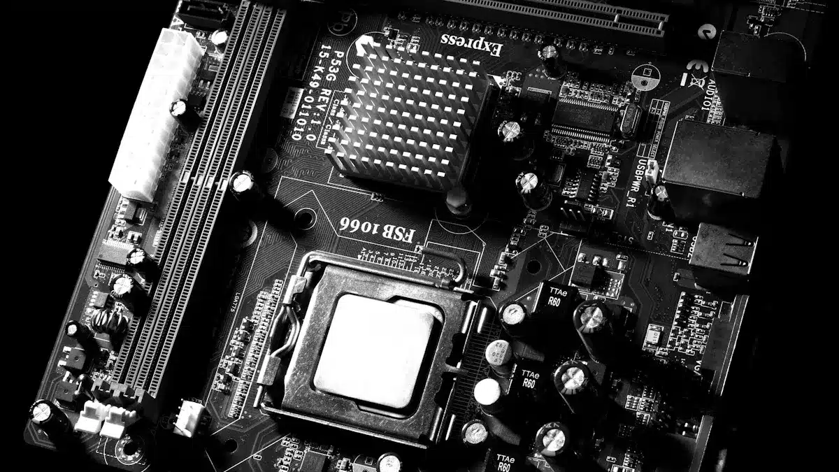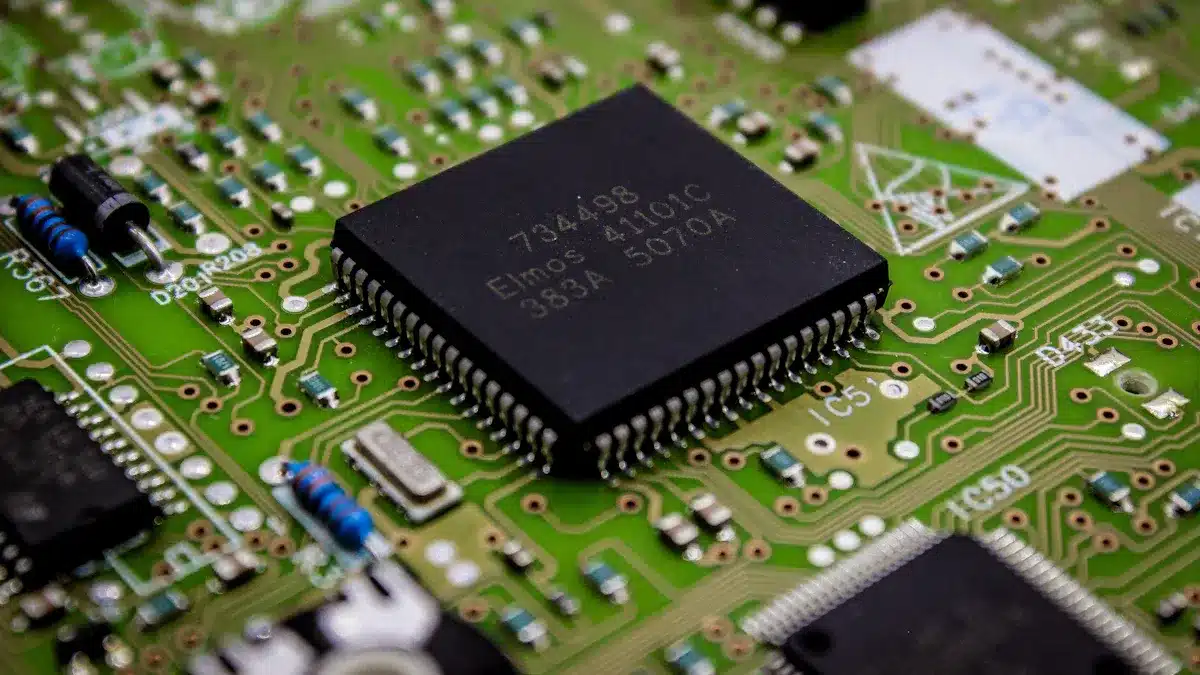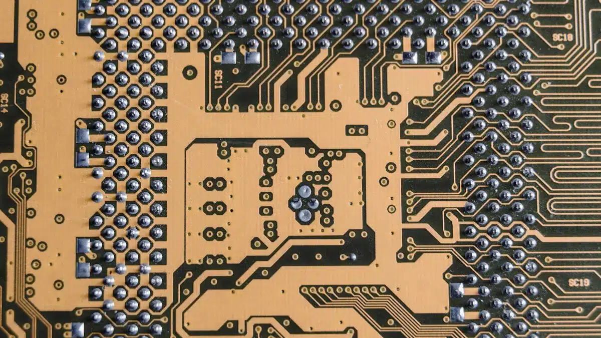
When you hear the term PCB, you might wonder, “pcb what does it mean?” PCB stands for printed circuit board. A printed circuit board acts as the backbone of most electronic devices. You use a circuit board to hold and connect electronic parts like chips and resistors. PCBs come in different types, such as rigid, flexible, and rigid-flex, to fit various needs. You might also see single-sided, double-sided, or multi-layer circuit boards in your gadgets. If you ever ask, “what are printed circuit boards?”—they are the platforms that let electricity flow between components, making your devices work.
Key Takeaways
A PCB, or printed circuit board, holds electronic parts and connects them. This helps devices work. PCBs have layers. There is a strong base. Copper paths carry signals. A protective mask covers the board. Labels help people put it together. There are different types of PCBs. Single-sided PCBs are for simple devices. Multilayer PCBs are for more complex devices. Flexible and rigid-flex PCBs can bend or are very tough. Making a PCB needs careful planning. People draw the design and test it. They check the quality to make sure it works well. This helps the PCB last a long time. PCBs make electronics smaller and lighter. They also make them more reliable. PCBs are used in things like phones, computers, and cars.
PCB: What Does It Mean

PCB Definition
You may wonder, “pcb what does it mean?” A printed circuit board is a flat board. It holds and connects electronic parts. Inside a device, you often see a green or blue board. This board has lines and dots on it. The lines are copper traces. The dots are pads for the parts. The printed circuit board gives your device its shape. It lets electricity move between the parts.
Printed circuit boards have layers of copper and insulation. Copper traces work like tiny roads for signals. The board supports everything and keeps parts in place. You use a circuit board to connect each part the right way. This setup makes devices smaller and easier to build. It also helps them work better.
Tip: If you ask, “what are printed circuit boards?”—they are the base that lets your phone, computer, or game console work.
Here is a simple table that shows the main parts of a printed circuit board and what they do:
PCB Component | Function |
|---|---|
Substrate Layer | Gives support and insulation, making the base of the PCB. |
Copper Traces | Work as paths that carry signals between parts. |
Solder Mask | Protects copper traces and stops short circuits. |
Silkscreen | Prints labels and symbols to help place and find parts. |
PCB Function in Electronics
You use a printed circuit board to connect and power parts. The main job of a pcb is to link parts so they work together. When you turn on a device, the pcb sends signals through copper traces. These signals carry data and instructions between chips and other parts.
Here are some important jobs of a printed circuit board in electronics:
PCBs are the main platform that connects and powers parts.
They let signals travel between parts so data and instructions move smoothly.
You can put resistors, capacitors, and inductors on the board for signal and voltage control.
Chips, transistors, and diodes sit on the board and help control current.
Connectors and interfaces let you link your device to other boards or gadgets.
Voltage regulators keep voltage levels steady.
Sensors and actuators help your device react or do things.
Printed circuit boards give support and connect parts. You solder parts onto the board. Copper traces make paths for signals. This setup answers, “what do pcbs do?” They help every part work together so your device works well.
If you look at a circuit board, you see how it brings parts together. Printed circuit boards replaced old wiring methods. Devices are now smaller and more reliable. You get a neat design that supports new technology.
Printed Circuit Board Structure

Layers and Materials
A printed circuit board is not just a flat piece. It has many layers, and each layer does something special. The main part is called the substrate. Most of the time, the substrate is made from FR-4. FR-4 is a strong material with fiberglass and epoxy. This makes the board tough and stops electricity from leaking. Some boards use polyimide for flexible designs. Others use metal cores to help with heat.
On top of the substrate are copper layers. These layers make paths for signals to move. Copper is used because it lets electricity flow easily. Usually, copper is put on both sides of the substrate. Over the copper is a green or blue solder mask. The solder mask keeps the copper safe and stops short circuits. The top layer is the silkscreen. The silkscreen shows labels and symbols to help you place parts.
The number of layers in a board can change how it works. Simple devices use one or two layers. Complex gadgets like computers use many layers. More layers let you fit more connections in a small space. They also help signals stay clear and avoid interference.
Note: Picking the right materials and layers helps your board last longer and work better.
Copper Traces and Pads
Copper traces are like highways on the board. Pads are like parking spots for parts. Traces are thin lines of copper that connect parts. They let signals move fast and safely. The width and layout of traces decide how much current they carry. Good design helps stop short circuits.
Pads are flat copper spots where you solder parts. Pads hold parts in place and let electricity flow. Good pads also help manage heat and keep the board cool.
Copper is used for both traces and pads. It carries electricity well and handles heat from soldering. How you place and size these features matters. Careful design keeps your device working well and stops signal loss or overheating.
Here is a quick table to show what each part does:
PCB Feature | Purpose |
|---|---|
Copper Traces | Carry signals between components |
Copper Pads | Hold and connect components to the board |
A good pcb uses the right materials, layers, traces, and pads. This makes sure your device works the way it should.
PCB Types
Printed circuit boards come in many shapes and sizes. You can pick from different types for your project. Each type has its own design and job.
Single-Sided and Double-Sided
Single-sided PCBs are used in simple things. These boards have copper on just one side. You see them in calculators, cameras, and audio gear. They cost less and are easy to make.
Double-sided PCBs have copper on both sides of the board. Vias are holes that connect the two sides. These boards are in LED lights, vending machines, and car dashboards. Double-sided boards let you add more parts and make harder circuits.
Here is a table to compare single-sided and double-sided PCBs:
PCB Type | Structure Description | Typical Uses | Cost and Complexity |
|---|---|---|---|
Single-Sided PCB | One copper layer on one side of the board | Calculators, cameras, audio | Lowest cost, simplest |
Double-Sided PCB | Copper layers on both sides, connected by vias | LED lighting, dashboards | Moderate cost, more complex |
Multilayer Printed Circuit Boards
You use a multilayer pcb for tough jobs. These boards have three or more copper layers. Insulation keeps the layers apart. Multilayer PCBs are in smartphones, computers, and medical tools. They help signals move well and keep things small.
Multilayer pcbs cost more and take longer to make. They give better signals and last longer. If you want a strong device, you need a multilayer pcb.
Tip: Multilayer PCBs are great for fast and reliable gadgets.
Flexible and Rigid-Flex
Flexible PCBs can bend and twist to fit small spaces. You find them in wearables, medical tools, and foldable phones. Flex boards save space and make things lighter. They can take the place of cables.
Rigid-flex PCBs mix stiff and bendy parts. You can fold or bend these boards without breaking them. Rigid-flex PCBs are used in planes, defense, and medical gear. They handle shaking and bumps better than normal boards.
Here is a quick list of pros and cons for flexible and rigid-flex PCBs:
Flexible PCBs:
Bend and twist to fit shapes
Save space and weight
Rigid-Flex PCBs:
Handle stress and shaking well
More complex and cost more
You can choose the best board by thinking about space, price, and strength. Each pcb type has special features for different jobs.
Circuit Board Manufacturing
PCB Design Steps
When you start a new circuit board, you follow a series of steps to turn your idea into a working product. You begin by choosing the right software for your pcb design considerations. Popular tools include Altium Designer, Autodesk EAGLE, and KiCad. These programs help you draw the electrical plan and arrange the parts.
Here is a simple list of steps you follow in pcb design:
Build a library of symbols and footprints for each part.
Draw the schematic by placing symbols and connecting lines.
Simulate the circuit to check if it works as planned.
Move the schematic to the layout tool.
Place each part on the board outline.
Draw copper traces to connect the parts.
Set design rules to make sure the board can be built.
Create files for manufacturing and assembly.
Tip: Always check your design for errors before sending it to production. This helps you avoid costly mistakes.
Production Process
After you finish the design, the production process begins. Manufacturers use your files to build the circuit board step by step. They start by laminating layers of copper and insulation to form the base. Next, they etch away extra copper, leaving only the needed traces. Drilling machines make holes for parts and connectors. These holes get coated with copper to link layers.
The next steps add a solder mask to protect the traces and a silkscreen for labels. Quality matters at every stage. Manufacturers use testing like visual checks, automated optical inspection, and in-circuit testing to find problems early. They also use x-ray and functional testing to make sure the board works as expected.
You see these steps in every pcb assembly, from simple gadgets to complex printed circuit board assemblies. High-quality materials and strict standards help your device last longer and work better.
Note: Careful testing and following industry rules ensure your circuit board meets safety and performance needs.
Importance of Printed Circuit Boards
Everyday Device Examples
You find printed circuit boards in many things you use. These boards help your electronics work well and stay safe. Here are some examples you might know:
Smartphones and tablets let you call, text, and play games.
Computers and laptops help you learn, work, and go online.
Televisions and gaming consoles give you fun at home.
Smartwatches and fitness trackers check your health and steps.
Kitchen tools like coffee makers, blenders, and microwaves help you cook.
Medical devices such as heart monitors and insulin pumps keep you healthy.
Security systems like door locks, smoke alarms, and cameras protect your home.
Cars use printed circuit boards for maps, music, engine, and screens.
You use these printed circuit board applications every day, often without thinking about them. These boards help make your devices smaller, lighter, and stronger.
Advantages of PCBs
Printed circuit boards have many good points over old wiring ways. You get smaller and lighter gadgets because PCBs use copper traces, not big wires. This design lets you fit more things into a small space. You also get better reliability since fixed parts stop loose wires and shorts.
PCBs help companies build devices faster and for less money. Machines put parts on the board with great care, so there are fewer mistakes. Clear labels and neat layouts make fixing and checking easier for workers. You are safer because PCBs handle heat well and cut down on electrical noise, which keeps parts safe.
Modern printed circuit boards help new tech like IoT and wearables grow. Flexible and packed boards let engineers make tiny, tough gadgets for hard places. These boards also help save power, so your battery lasts longer.
You can trust your electronics to work well because PCBs go through tough tests for strength and safety. Good design and strong materials help your devices last longer and work better. As tech gets better, printed circuit boards will keep making electronics smarter, safer, and more useful.
A printed circuit board, or PCB, gives shape and connects parts in your devices. PCBs help make electronics smaller and more dependable. They also make them easier to put together. You can find PCBs as thin green boards inside many gadgets.
TVs, game consoles, and car dashboards need them too.
When you learn about PCBs, you understand how your tech works. You also see why these boards are important in your life.
FAQ
What does PCB stand for?
PCB stands for “Printed Circuit Board.” You see these boards inside most electronic devices. They connect and support electronic parts like chips and resistors.
Can you repair a damaged PCB?
You can repair some PCBs if the damage is small. You might fix broken traces with solder or special wire. Large damage often means you need a new board.
Why do most PCBs look green?
Most PCBs look green because manufacturers use a green solder mask. This layer protects copper traces and helps you see the parts clearly.
How do you clean a PCB safely?
You can clean a PCB with a soft brush and isopropyl alcohol. Make sure you unplug the device first. Let the board dry before you use it again.
Are all PCBs rigid?
Not all PCBs are rigid. You can find flexible PCBs in devices that bend or fold, like wearables or foldable phones. Rigid-flex PCBs mix both types for special uses.
See Also
Understanding PCB Design And Its Importance In Electronics
Exploring The Meaning Of PCBA And Its Electronics Role
Defining PCBA And How It Functions In Electronics