
Electronic devices are all around us, from our phones to smart homes. A special part makes them work: the printed circuit board. Many people wonder, “What does PCB mean?” To answer that, what does PCB stand for in electronics? PCB stands for Printed Circuit Board. This basic part links and holds all the electronic pieces, making it the main component of almost every electronic item. The global market for printed circuit boards was valued at a significant 73.1 billion dollars in 2024, underscoring its immense importance. Every PCB ensures devices function correctly. Understanding what PCB means highlights its crucial role in today’s technology.
Key Takeaways
A PCB is a Printed Circuit Board. It is the main base. It is inside almost all electronic devices. It holds all the small electronic parts. It connects them too.
PCBs have layers. They are like a sandwich. These layers include a base. It is called a substrate. There are copper lines. They carry electricity. There is a solder mask. It protects things. There is a silkscreen. It is for labels.
PCBs make electronic devices small. They make them strong. They make them reliable. They help make many devices. They are made quickly. They are made cheaply.
There are different types of PCBs. Some are simple. They have one layer. Some have many layers. Some can bend. They fit in tight spaces.
What Does PCB Stand For: Definition
Printed Circuit Board: The Acronym
We talked about this before. What does PCB mean? It means Printed Circuit Board. This short name is for a key part. It is in almost all electronics. A printed circuit board is the main base. It holds electronic parts. It gives them structure. It connects them. This helps circuits work.
The Core Function of a PCB
A PCB is a basic part. It is like a backbone. It connects and holds parts. PCBs are key to most new electronics. They offer a place for parts. They connect them with electricity. This uses thin copper lines. These lines guide electric signals. They go between parts. These parts include resistors. They also include capacitors. And integrated circuits. PCBs put circuits right on the board. This makes things less complex. It saves space too. This is better than old wiring.
A PCB has a special material. It does not conduct electricity. It has lines printed on it. Or etched onto it. This base helps electricity flow. It goes between parts. PCBs usually have a stiff base. It does not conduct. But some are flexible. Or both stiff and flexible. Electronic parts attach to the board. These include diodes. Also inductors and transistors. Conductive lines act as wires. They connect these parts.
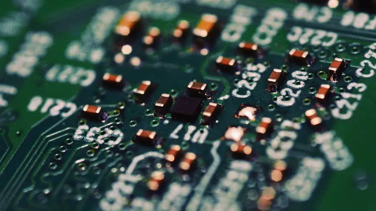
A normal PCB has four layers. They are pressed together with heat. From bottom to top, they are: the substrate, solder mask, silkscreen, and copper. The substrate does not conduct. It is often fiberglass. It is glued with epoxy resin. It often has fire protection. FR-4 is a common substrate. It is woven fiberglass cloth. It has epoxy resin in it. It does not soak up much water. It insulates well. It resists electric arcs. Other materials like aluminum are used. This is for parts needing much cooling. Flexible bases like Kapton are used. This is for flexible circuits. A thin layer of copper is on the substrate. This gives it electric and heat traits. A non-conductive layer is next. It is green solder mask ink. It is usually a polymer. Like epoxy resin. It is printed or sprayed on top. This makes a cover. Last, a silkscreen layer is added. It is usually white. It has letters and numbers. This helps with reading. It helps place parts. This careful PCB design makes it work.
It is key to know the difference. There is a bare PCB. And a PCB assembly (PCBA). A bare PCB is the main base. It is for electronic devices. It has a stiff base. It has etched copper lines. These make electric paths. It is an empty board. It has no electronic parts. Engineers use bare PCBs. They use them for new designs. For testing. And for teaching. They allow much design freedom. Engineers can change and test layouts easily. This is during development. No complex parts are mounted. This makes them good for new designs. And checking designs. Bare PCBs are also better. This is for small tests. And small production runs. They allow fast and cheap design changes.
A PCBA is different. It is a PCB with parts on it. These parts include resistors. Also capacitors. And integrated circuits. Workers solder them onto the board. They use Surface Mount Technology (SMT). Or Through-Hole Technology. A PCBA is a working board. It is ready for devices. Once a PCBA is put together. Its design is set. Changing it later is hard. And costly. PCBAs are vital for big production. Machines put them together. This ensures they are all the same. It is fast. And good quality. This is for thousands of units. This lowers the cost per unit. This is for big production. The main PCB functions come alive. This is with the parts. Knowing what PCB means helps make this clear. The whole PCB design guides both. It guides the bare board. And the final assembly.
PCB Anatomy: Layers and Components

A printed circuit board is like a sandwich. It has many layers. Some layers carry electricity. Some layers block electricity. Each layer has a special job. They all work together. This makes the PCB work. This smart design puts many circuits. They fit in a small space.
Substrate: The Insulating Base
The substrate is the main base. It is an insulating material. It does not let electricity pass. It makes the board strong. It keeps the electric layers apart. Fiberglass is common for stiff boards. FR-4 is a type of fiberglass. Flexible boards use polyimide films. Other materials are for special needs. Ceramic or metal cores are examples. Ceramic substrates use Alumina. Or Aluminum Nitride. These are for hot uses.
Copper Traces: Electrical Pathways
Copper traces are thin lines. They are made of copper. They act like tiny wires. They connect parts with electricity. Copper is a great conductor. It lets signals flow easily. There is very little resistance. This makes signals good. Copper conducts electricity well. This means signals move fast. It also saves energy. It stops heat from building up. This high conductivity helps. It allows thinner traces. This makes PCBs smaller. It also makes them cheaper. The PCB layout uses these traces.
Solder Mask: Protection and Color
The solder mask is a cover. It protects the copper traces. It stops short circuits. It also keeps copper safe. It prevents rust and damage. This layer is usually green. But it can be other colors. Red, blue, or black are common. Liquid Photoimageable Solder Mask is common. It is a liquid polymer. Makers put it on by printing. Or by spraying. It is very clear. It sticks well. It blocks electricity well. It also resists chemicals.
Silkscreen: Component Identification
The silkscreen layer is on top. It is above the solder mask. It is usually white. It has labels and marks. These marks help find parts. They also show direction. They show test spots. And company logos. This ink does not conduct electricity. It is epoxy-based. It is different from regular ink. White is most common. Yellow and black are also used. Screen printing is a common way. It puts on the silkscreen. Liquid Photo Imaging is more exact. Direct Legend Printing uses inkjet. It is fast and precise. This layer helps when building. It also helps when fixing. It makes PCB functions clear.
How a PCB Works: Electrical Connections

A printed circuit board (PCB) is like a brain. It helps electronic devices work. It moves electricity. It links all parts. This lets the device do its job. Good pcb design makes this happen.
Guiding Current: The Role of Traces
Copper traces are small paths. They are on a PCB. They move electric signals. They go between parts. These traces are like tiny roads. They replace old wires. Their size is important. This includes width and thickness. These control how much power flows. This stops overheating. It keeps signals strong. Copper traces are paths. They are on the pcb surface. They link parts like resistors. Also capacitors. And integrated circuits. This lets electric signals move. The pcb layout plans these links. This helps the device work. It sends signals and data.
Component Mounting: Secure and Functional
Electronic parts must stick well to the pcb. Two ways do this. Surface Mount Technology (SMT) puts parts right on the board. This way uses smaller parts. It makes designs compact. Through-Hole Mounting puts part leads through holes. Workers then solder them. This way is very strong. Other parts also hold the pcb. Screws, nuts, and standoffs hold it. They keep the pcb in its case. Standoffs lift the pcb. This lets air flow. It stops short circuits. These ways make sure the pcb functions well.
Multi-Layer Interconnectivity
Many PCBs have layers. These layers must connect. Vias are small paths. They are copper-plated holes. Vias link layers in a pcb. They move electric signals. This makes circuits smaller. It makes them complex. Through-hole vias are common. They go from top to bottom. They are drilled through the board. Then, they are plated. This makes a path. Vias are like vertical traces. They let signals flow. They go through tiny tunnels. This is key for advanced pcb design.
Why PCBs Are Essential in Electronics
Printed circuit boards are very important. They help make small devices. These devices are also powerful. They work well. They can be made in large numbers.
Enabling Miniaturization and Density
PCBs make devices smaller. They also make them stronger. Engineers use smart ways to do this. They stack parts closely. This is called 2.5D and 3D IC packaging. HDI PCB design helps too. It uses tiny holes. This makes more room for wires. It makes the board small. Designers also think about 3D shapes. These use space well. They stack parts up. Advanced packaging puts many functions together. This makes small parts. Smaller parts are chosen. Surface mount parts are used. They replace bigger parts. Multi-layer PCBs stack circuits. This makes them work like many boards. But in a small space. This careful PCB design makes things tiny.
Enhancing Reliability and Performance
PCBs make electronics work better. They keep signals steady. They stop interference. A shared ground stops noise. Ground planes act like shields. They stop changes in power. Ground vias help power flow back. This is good near noisy parts. Special connectors match the PCB. This helps signals move smoothly. Short wires stop reflections. Capacitors stop power spikes. They are near power pins. A good power network uses wide wires. This lowers resistance. Good layer design helps. It uses power and ground layers. This stops bad signals. Wires are kept apart. This stops crosstalk. Vias are put in pairs. They have a ground via. This helps current return. It stops signal problems. These PCB design choices make things strong. They make them work well.
Facilitating Mass Production
PCBs help make many electronics. Making them is very efficient. Many boards are put on one big sheet. This is called panelization. They are made at the same time. This saves a lot of money. SMT uses special machines. They quickly place small parts. AOI checks for problems. It looks at placement or soldering. ICT checks if each board works. DFM makes sure designs are easy to build. DFT adds things to make testing easy. Prototyping makes small versions. This tests how they work. It finds errors early. These steps make many PCBs. They are cheap and good quality.
Types of PCBs and Their Uses
Different devices need different PCBs. Engineers pick a PCB type. It depends on what the device needs. This includes how complex it is. Also, its size and if it needs to bend.
Single, Double, and Multi-Layer Boards
Single-layer PCBs are simple. They have one layer. It carries electricity. They are easy to make. But they have little space. Wires and parts can get crowded. This simple design can cause problems. It can make electric noise. Wiring signals on one layer is hard. They are used in LED lights. Also in calculators. And coffee machines. They are in solid-state drives. And other home electronics.
Double-layer PCBs have two layers. They carry electricity. They allow harder circuits. They make more connections. Multi-layer PCBs have three or more layers. These layers are stacked. They offer the most parts. They are the most complex. This makes small, strong devices.
Flexible and Rigid-Flex PCBs
Flexible PCBs can bend. They use special materials. These include polyimide and polyester. These materials block electricity well. They also handle high heat. Copper is the main material. It conducts electricity well. It is also strong. Glues like epoxy join layers. A cover protects the copper. It keeps out water and dust.
Making flexible PCBs has steps. First is circuit design. Then material is ready. Circuits are printed. Parts are placed. They are soldered. Testing makes sure it works. Flexible PCBs have many good points. They fit odd shapes. They save space. They save weight. This is key for smartwatches. And medical tools. They can replace big wires. This means fewer connections. It makes them more reliable.
High-Density Interconnect (HDI) Boards
HDI PCBs put more parts. They fit in a small space. They have tiny holes. These are called microvias. They also use blind vias. And buried vias. These boards have thinner lines. They have smaller spaces. They have smaller holes. They have smaller pads. This allows many connections. HDI PCBs use new methods. These include laser drilling. And stacking layers. These make more wires. They do not lose power.
HDI boards have many circuits. They are in a small area. They send signals fast. They make boards smaller. They make them lighter. This makes them work better. It helps with heat. HDI PCBs are key in many devices. These include smartphones. Also tablets. And smart wearables. They are in phone gear. And car systems. And medical tools. This PCB type makes small designs. It gives advanced features.
The printed circuit board is very important. It is the hidden base. It is in all electronics. It makes things work. It makes them small. It makes them reliable. New ideas keep making PCBs better. High-power PCBs handle more electricity. Flexible PCBs allow new designs. New materials help 5G work. AI makes PCB design better. It is faster. It is more efficient. These changes will make IoT devices smaller. They will connect better. Future PCB tech will have smarter designs. It will use earth-friendly materials.
FAQ
What is the main purpose of a PCB?
A PCB holds electronic parts. It connects them. It uses copper lines. These lines are like tiny wires. This makes devices small. They also work well. The PCB is the base. It is for all new electronics.
What is the difference between a bare PCB and a PCBA?
A bare PCB is an empty board. It has no parts. A PCBA is a PCB with parts. All parts are soldered on. It is a working circuit. It is ready for a device.
Why do some PCBs have multiple layers?
Multi-layer PCBs make circuits complex. They fit in small spaces. They stack many layers. These layers carry electricity. They are separated by insulation. This design adds more parts. It makes signals better. It is key for advanced electronics.
What is the function of the solder mask on a PCB?
The solder mask is a cover. It is usually green. It protects copper lines. It stops short circuits. This happens when soldering. It also keeps copper safe. It stops rust and damage.
Can a PCB be flexible?
Yes, PCBs can bend. They use special materials. These materials let them flex. Rigid-flex PCBs have both. They have stiff and bendy parts. This helps devices. They need small, moving connections.
See Also
Understanding PCBA: Its Abbreviation and Critical Role in Electronics
Essential Acronyms and Terminology for PCB and PCBA Explained
Decoding PCBA: Its Significance and Function in Modern Electronics
Exploring PCBA’s Definition and Vital Contribution to Electronics
PCB Design Fundamentals: Why It’s Crucial for Electronics Development