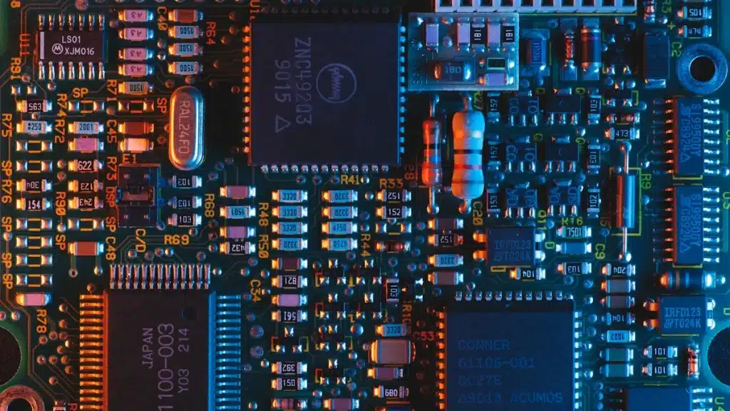

PCB fabrication assembly plays a crucial role in the electronics industry. PCB fabrication involves creating the physical boards, which serve as the foundation for electronic devices. This process ensures that the boards are durable and function properly. On the other hand, PCB assembly focuses on placing and soldering components onto these boards, making them operational. Understanding pcb fabrication assembly is essential for anyone involved in electronics manufacturing. The global PCB assembly market was valued at approximately USD 73.1 billion in 2023 and is projected to grow significantly as demand for advanced electronic devices increases.
Key Takeaways
PCB fabrication makes the basic circuit board. It does this by layering materials, etching copper, drilling holes, and adding protective layers. This creates a strong base for electronics.
PCB assembly puts and solders electronic parts onto the board. This turns it into a working device that is reliable and lasts a long time.
Both fabrication and assembly need careful steps and strict quality checks. This ensures the final product works well and avoids expensive mistakes.
Working with companies that do both fabrication and assembly can speed up production. It can also lower costs and improve product quality.
New technologies like AI, 3D printing, and automation are changing PCB manufacturing. They make it faster, smarter, and more efficient.
PCB Fabrication Overview
PCB fabrication is how we make printed circuit boards (PCBs) from design plans. This step is very important. It changes electronic designs into real boards that work. These boards are the main support for electronic devices. They provide mechanical strength and electrical connections. Knowing about the PCB fabrication process helps you see how complex and precise electronics manufacturing is.
PCB Fabrication Process Steps
The PCB fabrication process has several key steps:
Design and Layout: Engineers use computer-aided design (CAD) software to make a detailed design. This design shows where traces, pads, and components go.
Material Selection: Picking the right materials is very important. Common materials include FR-4, a strong fiberglass epoxy laminate known for its durability and electrical features.
Imaging: The design is put onto the substrate using photolithography. This step uses a light-sensitive film and UV light to create the pattern.
Etching: Unwanted copper is taken away using chemical etching. This leaves the circuit traces behind.
Drilling: Holes are drilled for vias and component leads. Precision is very important to make sure everything lines up correctly.
Plating: The drilled holes are coated with copper to make electrical connections between layers.
Solder Mask Application: A protective layer is added to stop solder from connecting traces during assembly.
Silkscreen Printing: Labels and markings are printed on the board to help with identification and assembly.
Final Inspection: Quality control checks, like Automated Optical Inspection (AOI), make sure the boards meet standards before they are shipped.
These steps show how detailed the PCB fabrication process is. Each stage needs precision and care to make sure the final product works well.
Importance of PCB Fabrication
PCB fabrication is very important for many reasons:
Foundation for Electronics: The made PCB is the mechanical and electrical base for all electronic devices. Without a good board, the device cannot work.
Impact on Performance: The quality of the fabrication process affects how well the final product works. Mistakes during fabrication can cause electrical problems, like short circuits or open circuits, which can ruin device function.
Quality Control: Using strict quality control during fabrication helps avoid mistakes. Common practices include:
In-Circuit Testing (ICT) to find open or short circuits.
Flying Probe Testing to check for loose connections and component problems.
Functional Testing to confirm the PCB works in real-life situations.
Cost Efficiency: A good fabrication process lowers the chance of mistakes, reducing rework and recalls. This efficiency can greatly cut production costs.
PCB Assembly Overview
PCB assembly is when we put electronic parts on a printed circuit board (PCB) and solder them. This step changes the bare PCB into a working electronic device. You can think of PCB assembly as the last step in making the product. Here, all the parts come together to create something that works. Knowing this process is very important for anyone in electronics. It affects how well the final device performs and how reliable it is.
PCB Assembly Process Steps
The PCB assembly process has several key stages:
Preparation Before PCB Assembly: This means checking the PCB design and doing Design for Manufacturability (DFM) checks. These checks make sure the design is ready for production.
Stencil Creation for Solder Paste Application: A stainless steel stencil is cut with a laser to match the PCB pad layout.
Solder Paste Application: Automated screen printing puts solder paste exactly on the PCB pads.
Component Placement: Machines pick and place components correctly on the board.
Reflow Soldering: The PCB goes through a reflow oven to melt solder paste and make solid connections.
Optical Inspection: Automated Optical Inspection (AOI) looks for surface problems like missing or misaligned parts.
Statistical Process Control: Quality data checks help improve assembly consistency.
X-Ray Inspection: This is used for complex parts to check hidden solder joints.
Selective Soldering for Through-Hole Components: Solder is applied to THT leads using special equipment.
Final Inspection and Handling: Visual checks, functional tests, cleaning, and packaging are done.
Feedback Collection: Feedback after delivery helps improve manufacturing.
Each step needs precision and careful attention. Automated systems help make the assembly process efficient and accurate.
Importance of PCB Assembly
PCB assembly is very important for many reasons:
Functionality: Good assembly connects parts and makes sure they work well together. This connection is key for how well the electronic device works.
Protection: The assembly process also keeps parts safe from things like moisture, dust, and chemicals. These can cause damage over time.
Reliability: Advanced assembly methods, like Surface Mount Technology (SMT), make devices more reliable. SMT allows for smaller parts and more connections, which are important for modern electronics.
Quality Control: Strict quality control steps, including automated checks, find problems early. This ensures only working boards move on to the next production stages.
Longevity: Well-made PCBs can last 15-20 years if handled properly. Bad assembly can cause early failures, affecting how long the electronic product lasts.
PCB Fabrication Assembly Relationship
Knowing how PCB fabrication and assembly relate is very important for anyone in electronics manufacturing. Both processes are different, but they work together to make electronic devices that function well.
Key Differences Between Fabrication and Assembly
The differences between PCB fabrication and assembly are big. Here’s a quick comparison:
Aspect | PCB Fabrication | PCB Assembly |
|---|---|---|
Process | Making the bare board: layering materials, etching copper traces, drilling holes, and adding solder mask and silkscreens. | Attaching and soldering electronic parts onto the made board. |
Equipment | Precision drilling machines, photolithography setups, and chemical etching stations. | Pick-and-place machines, solder paste printers, and reflow ovens. |
Required Expertise | Knowledge of materials, chemical processes, and precision machining. | Knowledge of circuit design, soldering methods, how components work, and testing techniques. |
Quality Control | Visual checks, electrical tests, and environmental tests. | Automated Optical Inspection (AOI), X-ray inspection, and functional tests. |
Challenges | Material defects, alignment problems, and etching mistakes. | Misplaced components, soldering problems, and thermal stress. |
Supporting Files | Gerber files for fabrication. | Bill of Materials (BOM) for assembly. |
Real-World Examples
Real-world examples show how PCB fabrication and assembly work together for successful product launches. For example, FastTurn offers complete solutions that include everything from multilayer PCB fabrication to complex SMT assembly. Their certified facilities make sure products are high-quality and ready for production.
Take TechInnovate, a startup in smart home devices. They had issues with quality and lead times when they used separate processes for PCB fabrication and assembly. By working with a complete provider, they improved their design for manufacturability. This change cut lead times from 10-12 weeks to just 4-5 weeks, reduced costs by 23%, and lowered defect rates. This teamwork between fabrication and assembly speeds up time-to-market and improves product success.
Another example is a startup making wearable fitness trackers. They used PCB assembly prototyping to quickly test designs and check component integration. This faster process helped them launch their product sooner, giving them an advantage.
These examples show how important it is for PCB fabrication and assembly to work together. Their relationship directly affects product quality and efficiency.
Future Trends in PCB Fabrication and Assembly
The future of PCB fabrication and assembly looks bright. New technologies and creative methods are leading the way. Several trends will change the industry in the next few years.
High-Density Interconnect (HDI) PCBs are becoming popular. They let makers use microvias and many layers. This helps create smaller and more powerful devices that fit today’s needs.
Additive manufacturing (3D printing) is changing how PCBs are made. It builds them layer by layer. This cuts down on waste and speeds up testing. This method allows for complex designs at lower prices.
Artificial intelligence (AI) is changing how things are made. AI helps plan production and improves quality checks. It also allows for custom PCB solutions by managing complex design details well.
Automation and robotics are making things more precise and scalable. Machines can do repetitive tasks, making work faster and cutting lead times. For example, robotic inspection systems use high-quality cameras to find defects, ensuring top-quality PCBs.
Quick turn PCB fabrication and assembly greatly affect how products are developed. This method shortens wait times, so you can get fully assembled PCBs in days instead of weeks. Here are some benefits:
You can quickly test and prototype designs, speeding up time-to-market.
Quick turn services help with small production runs, allowing market testing and faster feedback.
These services keep high-quality standards through strict quality checks.
You can quickly adjust to design changes, taking advantage of market chances.
As the PCB assembly market grows, expected to reach about USD 145 billion by 2032, demand for high-quality PCBs will rise. The growth of IoT, automotive electronics, and 5G technology will drive this change. Following these trends will help you stay competitive in the fast-changing electronics world.
In conclusion, both PCB fabrication and assembly are very important in making electronics. Here are the main points:
PCB fabrication makes the empty board with copper lines and holes.
PCB assembly adds and solders parts to make the board work.
Each step needs special skills, tools, and quality checks.
When you think about your needs in PCB manufacturing, look at things like experience, quality checks, and testing choices. Use this table to help you:
Assessment Factor | Explanation |
|---|---|
Experience | Pick companies that have a good history of being reliable. |
Quality Evaluation | Look at certifications and customer reviews to judge product quality. |
Testing Options | Make sure there are complete testing services available. |
Knowing these processes will help you make smart choices and improve your project results.
FAQ
What is the difference between PCB fabrication and assembly?
PCB fabrication makes the empty circuit board. Assembly adds and solders parts onto that board. Both steps are needed to create working electronic devices.
How long does the PCB fabrication process take?
The PCB fabrication process usually takes 1 to 3 weeks. This depends on how complex the design is and how many orders there are. Quick turn services can make this time shorter.
What materials are commonly used in PCB fabrication?
Common materials are FR-4, which is a strong fiberglass epoxy laminate, and polyimide for flexible circuits. These materials are tough and have great electrical features.
Why is quality control important in PCB manufacturing?
Quality control makes sure that PCBs work well. It helps find problems early, which lowers the chance of failures in electronic devices.
Can I prototype PCBs before full production?
Yes, prototyping lets you test designs and how they work before full production. This step helps find problems and improve your product for better performance.
See Also
A Clear Overview Of PCBA Manufacturing And Assembly
The Importance Of PCBA Services In Electronics Production
The Value Of Custom PCBA Manufacturing For Today’s Electronics